Lecture
Main functional units
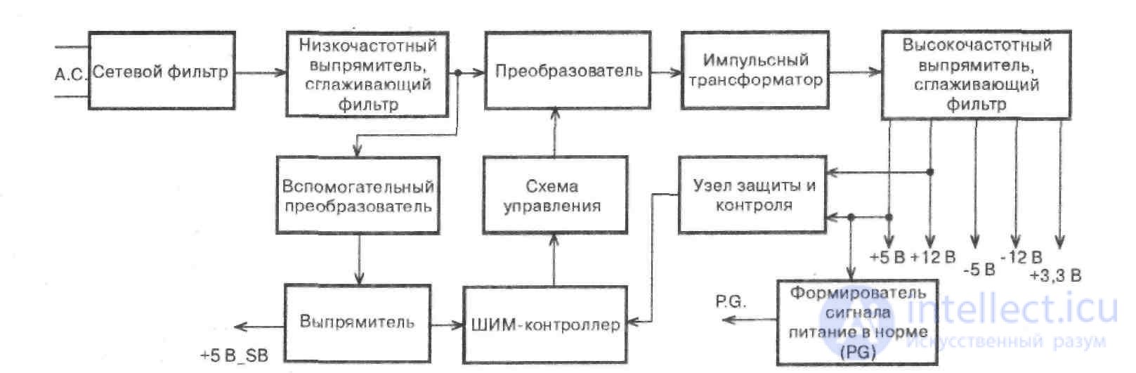
To understand the operation and structure of the power supply of the system module, the block diagrams of typical AT / ATX sources are given below and the operation of the most complex block structure node - half-bridge converter is explained. Block diagrams of AT, ATX power supplies are presented in Figure 1.2 and 1.3.
Power Supply AT / ATX Power Supply AT Power Supply
In an AT format power supply (Figure 1.2), the supply voltage through an external circuit breaker located in the system unit's chassis is fed to a line filter and a low-frequency rectifier. Next, the rectified voltage magnitude order 300 AT, half-bridge converter is converted into a pulse.
The isolation between the primary network and the consumers is made by a pulse transformer. The secondary windings of the pulse transformer are connected to high-frequency rectifiers + 12 V and ± 5 V and corresponding smoothing filters.
Power Good signal (power OK), supplied to the motherboard through 0.1 ... 0.5 with after the appearance of the supply voltage +5 V, performs the initial installation of the processor. The failure of the power part of the source is prevented by the node of protection and blocking. In the absence of emergency operation, the operation of these circuits form signals that allow the operation of the PWM controller, which controls the half-bridge converter by means of a matching cascade. In emergency operation mode, the PG signal is reset.
Maintaining the output voltages at a constant value in the controller is provided by the feedback control system, with the deviation of the output voltage from the +5 V and + 12V source as an error.
ATX power supplies
The ATX format power source (Figure 17) is distinguished by the presence of:
Functional elements
The section discusses examples of the practical implementation of the elements of the power supply circuit diagrams, as well as reference data for the main circuit elements and their analogues.
Input filter
The power supply is a serious source of computer interference for home TV and radio equipment [6, 7]. Causes of interference:
In order to prevent the penetration into the electrical network of impulsive noise generated by the power source, as a rule, a barrier filter is turned on at its input.
In addition to noise suppression, the filter, as an input element, also performs a protective function in emergency operation of a power source - current protection, overvoltage protection.
In some power supply circuits, the filter includes a nonlinear varistor element designed to limit the charging current of the high-voltage capacitive filter. In this paragraph we consider only those measures that are used to protect against interference at the input of the power source.
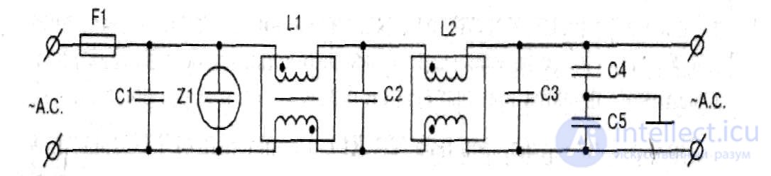
Typical barrier filter circuit
A typical diagram of the barrier filter of the power supply of the system module (Figure 18). At the input of the filter, capacitor C1 is turned on, then the AC mains supply voltage is supplied to the power supply unit of the system module through a network inductive-capacitive filter.
Current protection is provided by fuse F1, which limits the load current to no more than 1.25 of the nominal value, and from overvoltage (overvoltage) is provided by varistor Z1. When the supply voltage rises above a certain level, the resistance of the element Z1 decreases sharply, causing the fuse to trip.
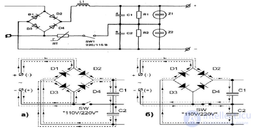
Low frequency rectifier
The inverters are powered by a constant voltage, which is produced by a low-frequency rectifier (Figure 19 ). The bridge rectification circuit, made on diodes D1 ... D4, ensures proper quality of rectification of the mains voltage. Subsequent smoothing of the rectified voltage ripple is performed by a filter on the choke L1 and the series-connected capacitors CI, C2. Resistors Rl, R2 create a discharge circuit of capacitors CI, C2 after disconnecting the power supply from the network.
The possibility of supplying from 115 V is realized by introducing into the rectifier circuit a selection switch for the supply voltage. The closed state of the switch corresponds to a low supply voltage (-115 V). In this case, the rectifier operates according to the voltage doubling scheme, and the charging process will proceed as follows. Let at some instant of time at the input of a rectifier be positive
half period of mains voltage. This is equivalent to the action of an external source, on the terminal 1 of which there is a positive pole, and on the terminal 2 - negative. The charge of capacitor C1 will occur along the circuit:
+ U cem (terminal 1) → D 2 → L 1 → C1 → SW 1 → NTCR 1 → - (terminal 2).
When changing the polarity of the half-cycle of the input voltage will be the charge of the capacitor C2 in the circuit:
+ U cem (terminal 2) → NTCR 1 → SW 1 → C2 → D 1 → - U cem (terminal 1).
The output voltage corresponds to the total value of the voltage on the capacitors C1, C2.
One of the functions of the rectifier is to limit the charging current of the input capacitor of the low-pass filter, made up of elements that make up the rectifier device of the power supply. The need for their use is caused by the fact that the converter startup mode is close to the short circuit mode. The charging current of a capacitor when it is connected directly to the network can be significant and reach several tens to hundreds of amperes.
The use of NTCR1-type thermistors with negative TCRs (Figure 19), connected in series to the charge circuit of the capacitor, eliminates unwanted charging effects of the input capacitor of the low-pass filter. The thermistor has some resistance in the “cold” state, after passing the charging current peak, the resistor warms up and its resistance becomes 20 ... 50 times less. In high-quality power supplies varistors Zl, Z2 are used. Their use is explained by the need to protect the unit from overvoltage in the supply network.
Half Bridge High Frequency Converter
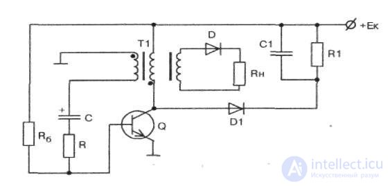
In the power supplies of the system modules, the high-frequency converter is made according to the two-stroke half-bridge type voltage converter circuit [6], the circuit diagram of which is shown in Figure 1.4. The active elements of the circuit are the transistor switches Q1, Q2 with back-on diodes Dl, D2. With the help of capacitors CI, C2, the diagram shows the capacitance of the collector-emitter transitions of transistors, mounting diodes, transformer T1, etc., and the voltage divider of the primary source EPIT is formed from capacitors C4 and C5. Elements D3, D4, Lf, Cf form an output rectifier.
The form of voltages in the collector Q2 (emitter Q1) is determined by the processes of energy accumulation in the primary winding of the transformer T1, the leakage inductance L $ and the charge (discharge) of capacitors CI, C2. If the transistor Q1 is open, the capacitor C1 is discharged through the open transition to the transistor Q1 and the charge of the capacitor C2, causing a voltage surge in the collector Q2 together with the action of inductance L $. In the case of an open transistor Q2, the capacitor C2 and the charge C1 are discharged, while in the emitter of Q1 there is a surge voltage due to the charge of this capacitor. On time diagrams (Figure 1.5), an increase in the charge current of capacitors C1 (C2) is observed, due to the increase in magnetization current T1. Capacitors C4, C5 in this circuit are the reactive equivalents of the bridge circuit transistors and close the current flow circuit through the primary winding T1.1.
Timing diagrams of voltages and currents
Transistor switches Ql, Q2 are open-ended and closed with phase signals U1 and U2 (see. Fig. 1.5), the time t0-t2 corresponds to the open state of the transistor Q1. In this case, the primary winding of the transformer T1.1 is connected to the output of the capacitive voltage divider C4, C5, as a result, the voltage on the locked transistors does not exceed the value of Epit / 2.
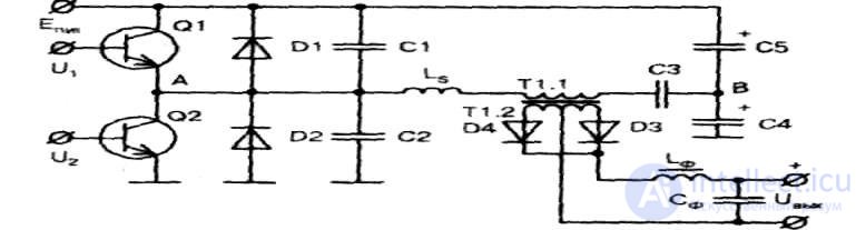
Two-stroke circuits are characterized by the phenomenon of "through currents", the cause of which is the inertia of the transition of the transistor from the on state to the off state due to the finite resorption time of excess minority carriers. The way to deal with through currents is to create a fixed delay of the opening signal relative to the closing one.
Auxiliary converter
Auxiliary converter is a design feature of ATX format power supplies. This converter generates a voltage of + 5BSB in the off state of the system module. The device is a blocking generator that operates in self-oscillating mode during the entire time of the closed state of the power switch of the power supply unit.
A simplified diagram of the self-oscillating blocking generator for the flyback converter is shown in Figure 21. The main elements of the blocking generator are the transistor Q and the transformer T1. The positive feedback circuit is formed by the secondary winding of the transformer, capacitor C and resistor R, which limits the base current. Resistor R $ creates a capacitor discharge circuit at the stage of the closed state of the transistor. Diode D prevents the voltage pulse of negative polarity arising when the transistor is locked into the load RH. A branch consisting of a diode D1, a resistor R1 and a capacitor C1 performs the function of protecting the transistor against overvoltage in the collector circuit.
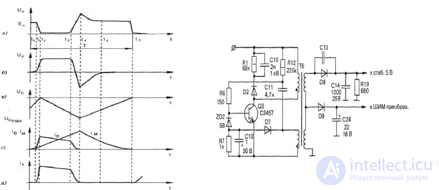
A typical autogenerator type converter circuit is shown in Figure 23. In all converter circuits, the key transistor operates in the mode with large switching current overloads of the collector, therefore, a powerful transistor is used in the autogenerator. To increase the duration of the “pause” of the key transistor in the auto-oscillatory mode, an additional source of negative bias is used. The emission control signal limitation is carried out by the ZD2 Zener diode, included in the base circuit of the key transistor Q3. In the damping circuit, it is permissible to use an RC circuit included in the collector circuit of the transistor, in some cases, the damping RC circuit is also installed in the key base circuit.
Output rectifier
Output power supply rectifiers are distinguished by the value of the output channel voltage. They are made according to the push-pull scheme and, as already noted, are available on UBbIX = +12 V, +5 V, -12 V and -5 V. Due to the high frequency of the converter, the use of special elements that allow operation at elevated frequencies and temperatures is explained. So, Schottky diodes with low voltage drop in the forward direction (0.2 ... 0.3 V for silicon diodes) and low-loss capacitors allowing operation at high temperatures are used as rectifier.
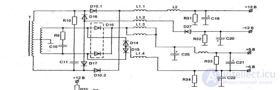
The output rectifier circuit of a typical ATX format power source is shown in Figure 24. The rectifier of each channel is made using a full-wave rectifier circuit with a lower ripple factor compared to single-half-wave. Filtering the output voltage of the output voltage is performed inductive (LI, L3, L4) and capacitive filters (C19, C20, C21, C22 and C25). The inclusion of serial RC-chains R9, CU and R10, SP parallel to the windings of transformers allows to reduce the intensity of the noise generated by the source. The possibility of a significant increase in the voltage at the rectifier output when the load is disconnected is eliminated by resistors R31, R32, R33, R34.
The rectifier +3.3 V of ATX format power sources (Figure 3.40) can be made according to the simplest serial compensation voltage regulator circuit, as for example in PM-230W.
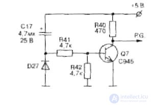
Power signal conditioners Good
To correctly start the computer’s computing system, a power supply delay is arranged in the motherboard until the transients in the power supply run out and the output voltages are established at the output. For this purpose, a special Power signal is generated in the power supply. Good ("food is normal"). The Power Good signal delayed by 0.1 ... 0.5 s represents the level of a logical unit, of the order of +5 V, which is intended for the initial installation of the motherboard.
Shapers can be made in discrete and integral design.
Chains of protection and control
Protection of power sources is manifested in critical operating modes, as well as in those cases where the action of feedback can lead to limiting modes of operation of circuit elements, thereby preventing the failure of power and expensive circuit elements.
As a result of the protection circuits, the output control signals from the PWM controller are removed, the transistors of the converter are in the off state, there is no output secondary voltage. It is necessary to distinguish such chains of protection:
The first two types of protection are close in action and are related to the prevention of high power to the load from the converter. They operate in case of overloads of the power supply or faults in the converter. Overvoltage protection can occur when input voltage drops and in some other cases.
The converter is turned off in the power sources by means of an additional error amplifier, usually an error amplifier 2 switched on by a comparator or via the pause control channel. Below are descriptions of the protection schemes for the power sources in question.


Comments
To leave a comment
Diagnostics, maintenance and repair of electronic and radio equipment
Terms: Diagnostics, maintenance and repair of electronic and radio equipment