Lecture
Node line scan (CP) in the VM is designed for:
The electron flux density and, accordingly, the brightness of the luminous dot on the screen are controlled by roughly setting the voltage value A3, smoothly by the adjustment available to the operator by varying the DC voltage supplied to the modulator, and modulating the brightness to obtain an image on the raster using AC or pulsed voltage on the cathode.
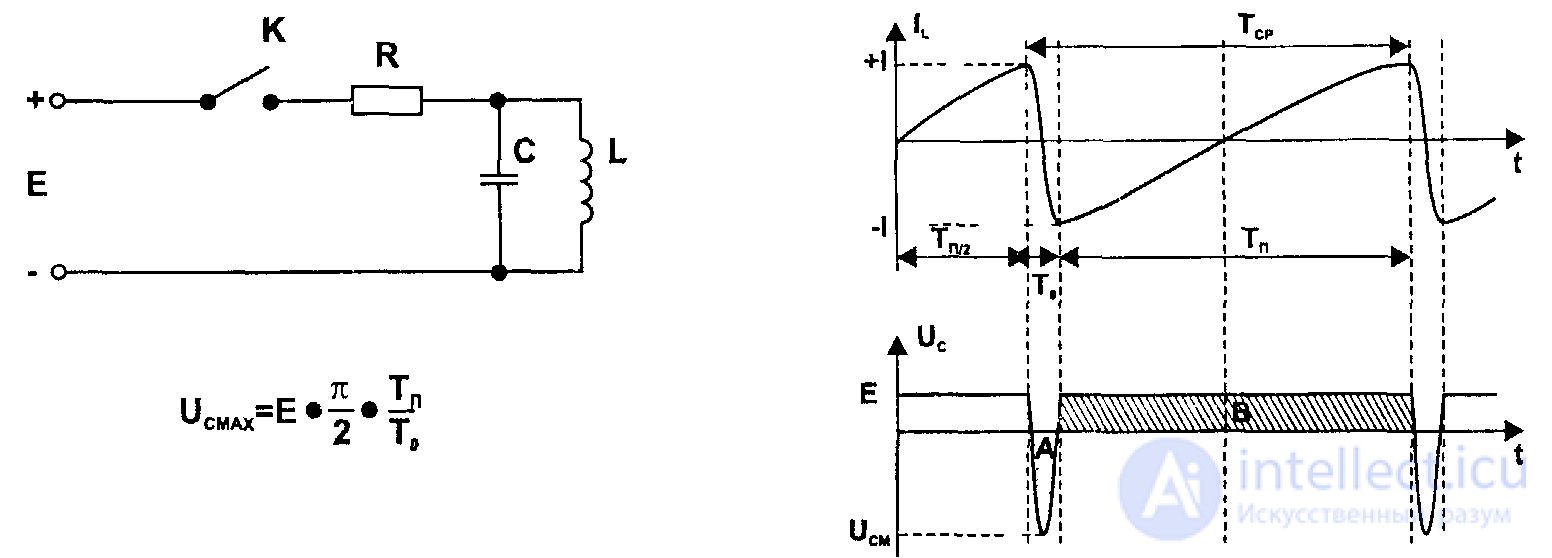
The principle of obtaining a sawtooth current in the horizontal deflecting coils consists in the formation of a linearly increasing current through the inductance of the coils when a rectangular voltage pulse is applied to them.
The idealized circuit used to implement this principle is shown in Figure 1, where L is the inductance of the lowercase OS coils, C is the own capacity of the coils, R is their resistance, and the form of voltages and currents in the circuit is shown in Figure 1, on the right.
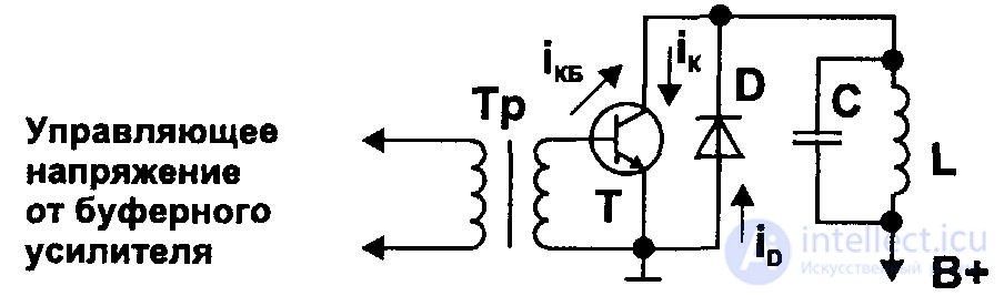
Typical scheme for obtaining sawtooth current works as follows. The control pulses from the line frequency master oscillator are amplified by a buffer cascade and fed through the matching transformer Tr to the base of the VT transistor. The positive voltage on the base corresponds to the open state of the transistor, and the negative closes it.
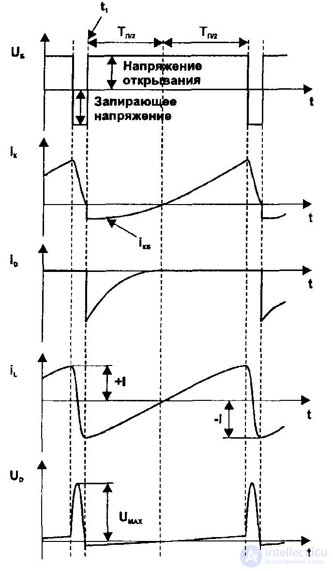
In the second half of the period of the direct course of the sweep, the current flows through the deflecting coils and the transition of the QE transistor, its growth stops by closing the transistor. At this moment, free oscillations occur in the oscillatory circuit of the LC, and after half of their period has elapsed, when the voltage Ud changes polarity, diode D opens, providing the key to conduct in a different direction.
At the same time, the current through the coils (i) also changes its direction and decreases from the maximum negative (-I) value to zero, at the same time the energy of the magnetic field stored in the coils returns to the power source. With a negative voltage at the collector, a certain current flows through the K – B junction of the transistor, therefore a total current equal to I = ikb + id flows through the coils.
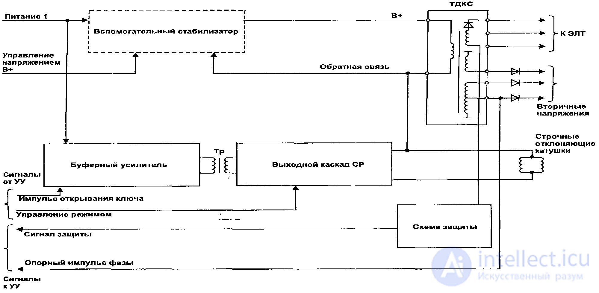
The outlined principles of the formation of a sawtooth current and obtaining high voltage are implemented in a typical block diagram of the horizontal scanning unit Figure63.
Diagnostics and repair of CP node
It is useful to diagnose the CP node before the first power up of the VM. Perform dusting of parts of the unit, and first of all, TDX
(Transformer Diode-Cascade Line)
Inspect the printed circuit board in the area of the power elements and simultaneously determine the conformity to the type of the block diagram, the method of switching on the key transistor and the damping diode, and also find out how the power is supplied to the circuit.
Check the state of the key transistor with an ohmmeter directly on its findings - the Q-E transition should not be damaged. (It should be borne in mind that a damping diode is connected parallel to the key transistor (or a two-diode diode modulator circuit), it can also be damaged, therefore, to make sure that the transistor is faulty, it is possible to drain the diodes. transistor replace.)
After replacing defective parts, check the absence of a short circuit. between the power supply of the primary winding and 0V ohmmeter directly at the terminals of the TDKS.
The presence of resistance less than 0.5 kΩ indicates damage in the TDKS or the additional voltage source B + circuit; a defect in the electrolytic capacitor of the filter is also possible.
Practically, this test is as follows. Disconnect the TDX B + power output from the power supply circuits on the printed circuit board by breaking the corresponding jumper in this circuit, or by dropping the filter choke normally present in the power supply circuit of the output stage, then connecting it to the power supply with a voltage of 12 - 24 V. This reduces the effect power dissipated by the transistor many times, - it will be below permissible even when working on TDKS with short-circuited coils. Then turn on the power and the oscilloscope controls the waveform on the collector of the key transistor - it should look like a sawtooth and should have a reverse pulse in the form of narrow positive half-wave sinusoids.
If, in the picture in question, there are other signals in the intervals between the backward pulses, resembling oscillations, this indicates the presence of short-circuited turns in one of the windings of the TDCC or insufficient current saturation in the base of the key transistor.
The found faults are eliminated by replacing the corresponding elements, after which they restore the circuit, i.e., remove the capacitors installed during the test, install soldered jumpers, etc.
At the final stage, the actions of all controls on the front panel of the unit are checked and the necessary trimmers on the board are adjusted. The necessary stage of checking the CP node is to control the thermal regime of the key transistor, preferably within one hour.

Comments
To leave a comment
Diagnostics, maintenance and repair of electronic and radio equipment
Terms: Diagnostics, maintenance and repair of electronic and radio equipment