Lecture
Introduction What is memory anyway?
All computer functions have common features
Data processing (CPU, GPU….)
Data storage (CDR, HDD, Memory…)
Data movement (FSB, PCI-E, USB….)
Control (North Bridge, South Bridge…)
Why memory improve performance?
CPU runs much more faster than HDD. If all data & application were stored in HDD. CPU will always wait for HDD to pass data
. Bottle neck in HDD, CPU idle most of the time
Memory enhance the usage of CPU.
Static RAM (SRAM)
Faster, more expensive
Need not to be recharged regularly like DRAM
Cache
Dynamic RAM (DRAM)
Less expensive, need to be refreshed
DRAM subtypes to be introduced
– Synchronous DRAM (SDRAM)
Please refer to SDRAM(New).ppt for details.
– Double Data Rate Synchronous DRAM (DDR)
Please refer to DDR (New).ppt for details.
– Double Data Rate 2 Synchronous DRAM (DDR2)
Please refer to DDR II(New).ppt for details.
– Rambus DRAM(RDRAM)
not being used anymore, not being discussed here.
Please refer to RDRAM(New).ppt for details.

SO-DIMM Type
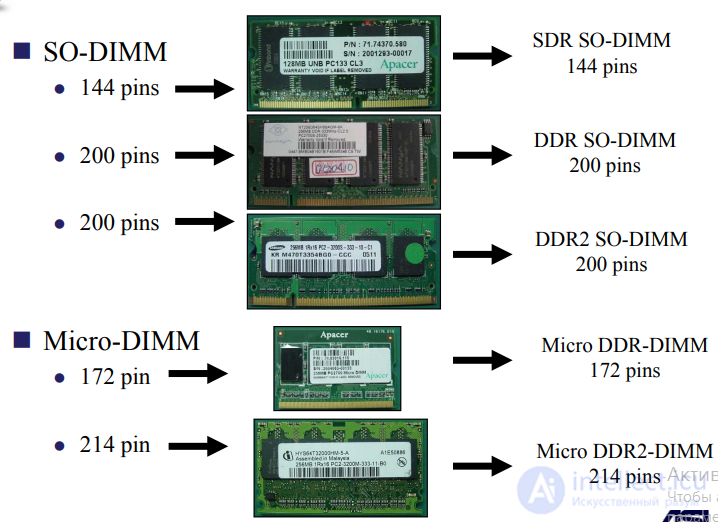
What memory looks like?

Performance related terms
Access Time (Nano seconds)
measuring from when the memory module receives a
data request to when that data becomes available.
lower numbers indicate faster speeds.
CAS latency
the number of clock cycles it takes before a column
can
be addressed on the DRAM chip.
Latency is a measure of delay
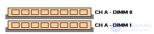
Dual channel mode
please refer to the picture next page.
MEMORY BANKS
Most computer systems have two or more memory banks –
usually called bank A, bank B
Error Correction Code (ECC)
data integrity checking method used primarily in high-end PCs
and file servers. Please refer to ECC(New).ppt for details.
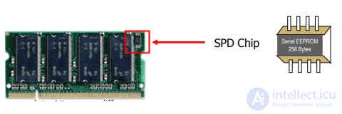
Serial Presence Detect (SPD)
store information about the memory module.
Please visit
http://www.webopedia.com/quick_ref/dram_memory.asp &
http://www.webopedia.com/Hardware/Memory/
When a computer is booted (started), serial presence detect
(SPD) is information stored in an electrically erasable
programmable read-only memory (EEPROM) chip on a
synchronous dynamic random access memory (SDRAM)
memory module that tells the basic input/output system
(BIOS) the module's size, data width, speed, and voltage
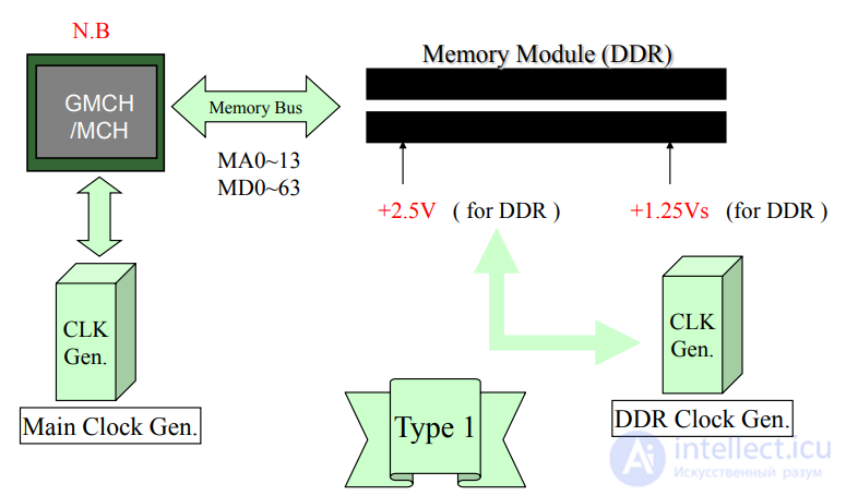
DDR BASIS
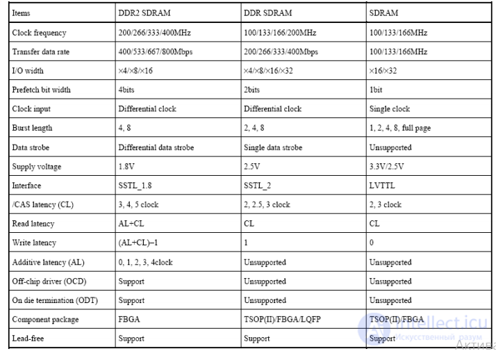
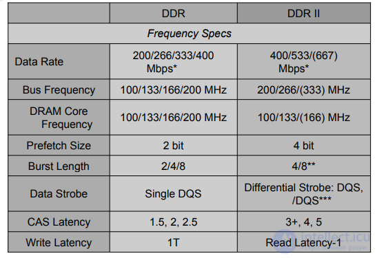
Short for Double Data Rate-Synchronous DRAM, a type of SDRAM that supports data transfers on both edges of each clock cycle (the rising and falling edges), effectively doubling the memory chip's data throughput.
DDR-SDRAM also consumes less power, which makes it well-suited to notebook computers. DDR-SDRAM is also called SDRAM II and DDRAM.
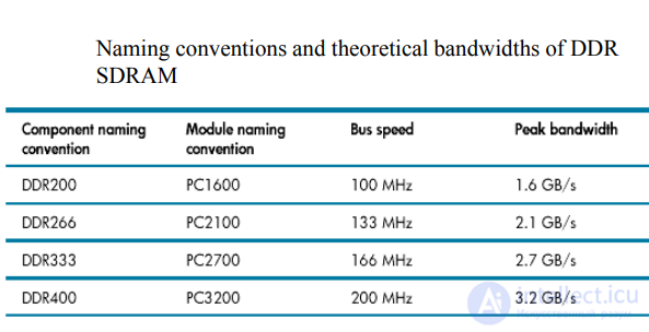
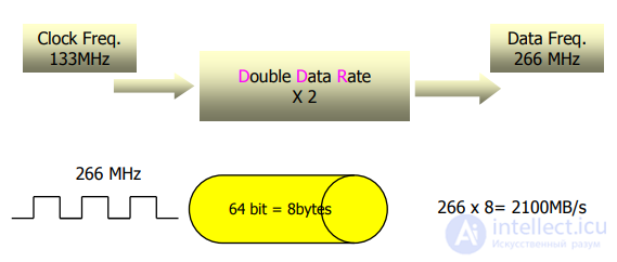
DDR 266 operating clock is 266MHz,if the data bus width is 64bit,in other word it’s 8bytes,thus DDR 266 memory bandwidth is 266MHz x 8=2100MB/s,i.e. PC 2100
PC1600 (DDR200)
100(MHz)×2×8(Byte) = 1.6GB/S
PC2100 (DDR266)
133(MHz)×2×8(Byte) = 2.1GB/S
PC 2700 (DDR333)
166(MHz)x2x8(Byte) = 2.7GB/S
PC 3200 (DDR400)
200(MHz)x2x8(Byte) = 3.2GB/S

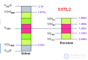
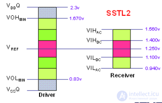
Double Data Rate IC's use 2.5 volt SSTL_2 compatible I/O [class II], how ever the supply voltage may be higher. The main supply voltage [VDD] is 3.3v or 2.5v for DDR 200, DDR266, and DDR333, while 2.6v for DDR400. The output drive supply [VDDQ] is 3.3v or 2.5v for DDR200, DDR266, and DDR333, while it's 2.6v for DDR400. DDR uses a bi-directional data strobe to indicate valid data [DQS].
STL-2: Stub Series Terminated Logic for 2.5v [JESD8-9]. Class II provides for higher power dissipation, Higher drive and a maximum current of 15.2mA. DDR, Double Data Rate. [JESD79] defines two data transfers per clock cycle. The Clocks are differential. Power Supply [VDD = 3.3v + 0.3v or 2.5v + 0.02v for DDR 200, DDR 266, or DRR 333; and 2.6v + 0.1v for DDR 400]. Inputs and outputs are compatible with SSTL_2. These DIMMs are 184 Pin in size and are not interchangeable with older 168 on SDRAM modules.
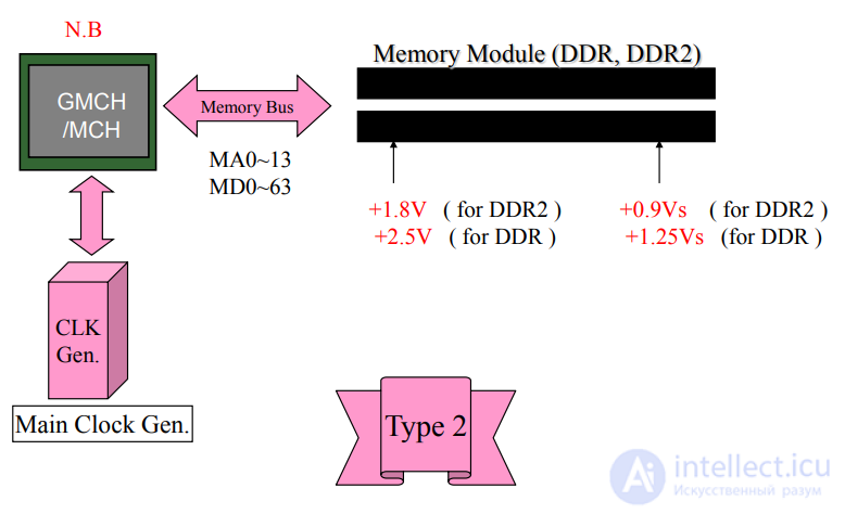
DDR2 SDRAM (Double Data Rate Two Synchronous Dynamic Random Access Memory)
The advantage of DDR2 over DDR SDRAM is its ability to run at much higher clock speeds due to an improved electrical interface.
Like DDR, DDR2 will transfer data on every rising and falling edge of the clock (double pumped), achieving an effective rate of 200 MHz with the same clock frequency
DDR2 DIMM memory modules are not backwardcompatible with DDR DIMM , due to incompatible pin configurations, core voltage, and memory chip technology.
DDR2 modules are designed with a different "key" in the edge connector to prevent insertion into incompatible memory sockets such as DDR motherboard. A DDR2 SDRAM DIMM will not fit into a standard SDRAM DIMM socket or a DDR DIMM socket.
DDR2 modules use a 1.8V power supply, providing a big power saving over the 2.5V DDR modules.
In this scenario, the core is running at 100 MHz, for DDR I, the I/O
buffers is synchronous with the core.
Only the protocol varies and in the case of DDR II, the I/O buffers
are clocked at twice the core frequency. In order to satisfy the
output
DDR I prefetches 2 bits, DDR II needs to prefetch four bits with
every read command and pipeline them for time multiplexed output
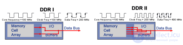
DDR vs. DDR II

The two channels handle memory-processing more
efficiently by utilizing the theoretical bandwidth of the two
modules, thus reducing system latencies, the timing delays
that inherently occur with one memory module.
Rules to Enable Dual Channel Mode
Matched DIMM configuration in each channel
Same Density (128MB, 256MB, 512MB, etc.)
Same DRAM technology (128Mb, 256Mb, or 512Mb)
Same DRAM bus width (x8 or x16)
All either single-sided or dual-sided
Double Data Rate II IC's use 1.8 volt SSTL_18 compatible I/O [class II], how ever the supply voltage may be higher. SSTL-18: Stub Series Terminated Logic for 1.8v [JESD 8-15A]. Class II provides for higher power dissipation, Higher drive and a maximum current of 15.2mA
DDR2 modules contain the require resistor termination located on the
memory chips using a technique called On-Die Termination [ODT].
While DDR1 modules have the necessary resistive termination located
on the motherboard. Using ODT, DDR2 are able to reduce the parts
count required for mother board while at the same time locate the
terminations closer the the signal destination. The ODT termination
can be turned on or off by the DRAM controller. Normally the
terminations are turned on for Writes and disable for Reads. The value
of the ODT termination is selectable based on the number of modules
in the system. With one DIMM module the ODT value is set at 150
ohms [300Ω pull-up and 300Ω pull-down]. When two modules are
loaded into the system the ODT value is changed to 75 ohms [150Ω
pull-up and 150Ω pull-down] for the DIMM not being written to while
the DIMM being accessed has its ODT turned off. Writing to the
Extended Mode Register [EMR] controls the ODT presence and value.
Three combinations are allowed; termination disabled, 75 ohms, and
150 ohms [ also 50 ohms]. The newest revision adds 50 ohm
termination values. ODT improves the eye-diagram over SSTL for
either Single-Rank or Dual-Rank modules.
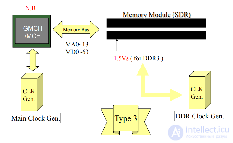
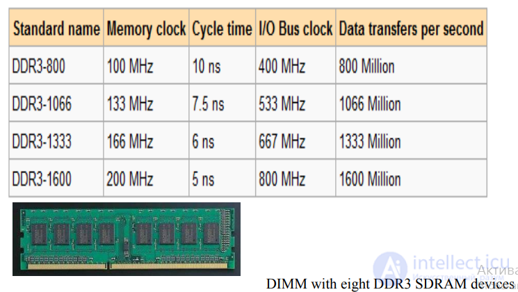
DDR 3
DDR3 SDRAM(Double Data Rate Three Synchronous
Dynamic Random Access Memory)
DDR3 SDRAM improves on DDR2 SDRAM in several
significant ways:
1.Higher bandwidth due to increased clock rate
2.Reduced power consumption due to 90nm fabrication
technology
3.Pre-fetch buffer is doubled to 8 bits to further increase
performance
4.The voltage of DDR3 SDRAM DIMM's was lowered from
1.8V to 1.5V. This reduces power consumption and heat
generation, as well as enabling more dense memory
configurations for higher capacities.
DDR3 SDRAM is normally packaged in DIMM modules


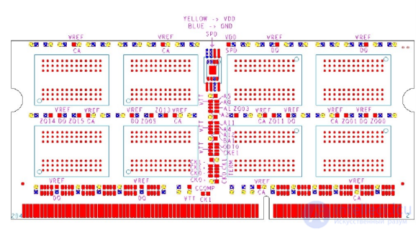
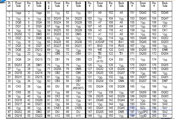
DDR SO-DIMM Signal Description
RAM Diagnostics and Troubleshooting Chart
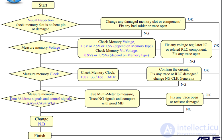
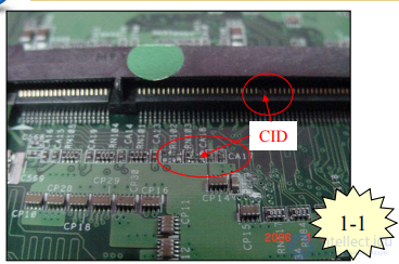
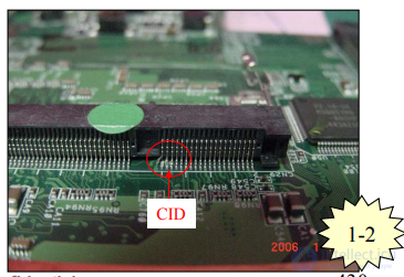
Visual Inspection
1.Check memory slot / Pin is not damaged or bent pin inside.
2.Check related resistor , capacitor component no damage. 3.Fix any trace open or BAD solder
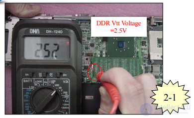
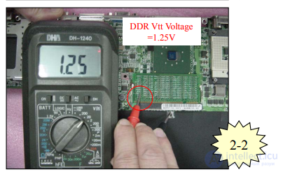
Use Multi-Meter or Oscilloscope to measure Memory Voltage & Vtt Voltage
. Memory Voltage: SDRAM: 3Vs DDR :2.5V
DDR2: 1.8V Memory Vtt Voltage: DDR :1.25Vs DDR2: 0.9Vs
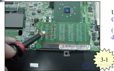
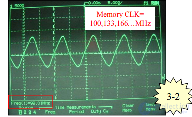
Use Oscilloscope to measure Memory Clock (100Mhz,133Mhz,166Mhz…depends on different chipset & memory)

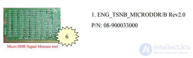
Plug Memory measure card into slot.
Use Multi-Meter to measure memory
signals’ bias voltage value. Compare
with good MB if you find any
unusual.


Comments
To leave a comment
Diagnostics, maintenance and repair of electronic and radio equipment
Terms: Diagnostics, maintenance and repair of electronic and radio equipment