Lecture
Это окончание невероятной информации про внешних факторов на надежность.
...
terminals, moving elements relative to the base, reducing contact and intercontact gaps.
The harmful effects of mechanical loads on the equipment are reduced by increasing the strength of the structure, using elements with increased mechanical strength, isolation of elements or equipment from mechanical stress (shock absorbers, packaging, etc.), rationally placing the equipment in containers and on objects.

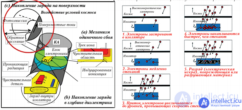
Fig. . Single failures in the operation of satellite electronics (SEE events - Single Events Effects) when high-energy protons and ions enter electronic components and the space charge of the satellite is created by high-energy electrons, which causes breakdown of dielectrics and disruption of on-board electronics [9-11]
When gamma and X-ray radiation (including secondary radiation, obtained due to collision of electrons with the apparatus body) passes through the microcircuit, the charge begins to gradually accumulate in the gate dielectric of the transistors, and accordingly the parameters of the transistors begin to slowly change - the threshold voltage of the transistors and the leakage current. An ordinary civilian digital microcircuit may already stop working normally after 5000 rad (however, a person may stop working after 500-1000 rad).
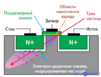
Fig. . Field effect transistor
In addition, gamma and X-ray radiation makes all pn junctions inside the microcircuit work like small “solar panels” - and if radiation in space is usually insufficient to greatly affect the microcircuit's operation, gamma and X-ray flux may already be enough during a nuclear explosion to disrupt the chip due to the photoelectric effect.
Failure mechanisms caused by single events are fundamentally different from failure mechanisms of the first kind. These failures can occur at any time, without requiring the accumulation of any dose. Such single events include recoverable failures - a change in the state of the memory register (SEU) or a short-term change in the level at the output of a logic element (SET), as well as catastrophic failures that lead to loss of system functionality either permanently or before the power is removed and restored. Catastrophic failures include SEL - transition of the microcircuit to a state with high current consumption due to the thyristor effect, SEFI - functional failure of the device due to a single event, SEB and SEGR - failure of the microcircuit or logic cell as a result of SEL.SHE - unrecoverable sticking of a trigger or memory cell in one state. Only the first two failures (SEL and SEFI) do not lead to a complete failure of the device and can be eliminated by turning off the power and rebooting. It is single failures that are sensitive to the size of the element, since the smaller the element, the less its volume and capacity and the less energy is enough to change its state.
Suppressing single failures is a more difficult task than fighting slow failures, since the total accumulated dose can be reduced by several orders of magnitude by shielding. Thus, an aluminum layer of 2 mm reduces the accumulated dose of cosmic radiation by a factor of 100 [10, 11], however, in order to reduce the dose by another two orders of magnitude, protection with a thickness of 8 mm is required. This paradoxical fact is easily explained by the fact that the composition of cosmic rays is heterogeneous. If low-energy particles, as a rule, are trapped in a thin screen, then high-energy particles can easily penetrate through it [12]. Therefore, the composition of the radiation behind the screen will radically differ from what it was in front of the screen, and in order to weaken this radiation flux, a much more thorough protection will be required.Heavy charged ions and elementary particles of high energies can interact with the screen material and generate secondary particles, sometimes even more dangerous for IP [13]. Experience shows that single events caused by cosmic rays or particles induced by them are observed even at sea level.
Methods for dealing with single failures are divided into two groups: the fight against SEL and its consequences (SEFI, SEB, etc.) and the fight against recoverable failures. To overcome SEL, it is necessary to form the topology of each element so as to avoid the formation of spurious transistors, which together with the main one can form a thyristor. A decrease in the supply voltage also contributes to an increase in the resistance of the IC to SEL, since if it is lower than the holding voltage of the parasitic thyristor, the latch will either not occur or will stop within a short time [14].
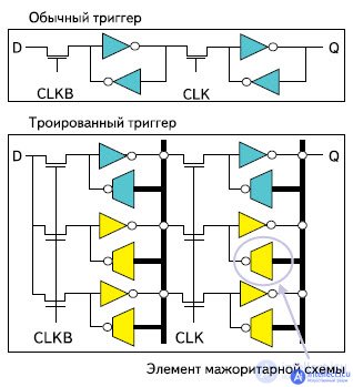
Fig. 2. The structure of the conventional and triple trigger
To combat the SEU, redundancy of memory cells is used (the so-called tripling - TMR) (Fig. 2). The essence of this approach to the design of ICs is that each register or trigger is replaced by three connected in parallel at the inputs and a majority circuit at the output. Since all triggers are combined by inputs, their outputs should always have the same levels (with the exception of transition times, if delays in triggers differ). If, as a result of the SEU, an incorrect level is established at one of the inputs, the majority circuit detects this and asynchronously returns the failed trigger to the correct state. In addition, her task is to form the output level of the cell, which is calculated by voting: which levels are greater at the outputs of the triggers, they set the state of the output.
Another way to deal with SEUs is to use FLASH, Antifuse, or C-RAM cells instead of SRAM to store rarely changed information. This protects against the SEU, since the energy required to change the state of such cells is much more than the energy required to throw the SRAM trigger [15].
Heavy charged particles (TZZ) - protons, alpha particles and high-energy ions
This is the biggest problem of space electronics - TZZs have such high energy that they “pierce” the microcircuit through (together with the satellite’s body) and leave a “loop” of charge . In the best case this can lead to a software error (0 become 1 or vice versa - single-event upset, SEU), in the worst case it can lead to thyristor latching (single-event latchup, SEL). In a latched chip, the power is shorted to ground, the current can go very large, and lead to the burning of the chip. If you manage to turn off the power and connect it before combustion, then everything will work as usual.
There are several ways to deal with snapping:
1) Monitor the current consumed, and quickly distort the power
2) Use microcircuits on a sapphire substrate (Silicon-on-sapphire, SOS, in a more general form Silicon-on-insulator, SOI) - this eliminates the formation of bipolar parasitic transistors and correspondingly snapping. Nonetheless, there may still be software errors. Silicon-on-sapphire wafers are expensive, difficult to process, and they have limited use in the civilian sector - accordingly, production is expensive.
3) Use the so-called triple-well process - it also greatly reduces the possibility of snapping the microcircuit due to the additional isolation of transistors by the pn junction, but does not require any special plates or equipment and, accordingly, the production itself is much cheaper than silicon on sapphire.
Neutrons + 10B
Boron is used for doping silicon and in the form of borosilicate glass to isolate metal layers. The problem is that natural boron for 20% consists of Boron-10, which reacts very well with neutrons with the release of alpha particles directly in the heart of the chip. This led to errors in the operation of microcircuits, especially memory.
Neutrons are obtained as secondary radiation, or fly from the earth, as we recall in space radiation they are not.
10B + n → [11B] → α + 7Li + 2.31 MeV.
This is one of the problems that we managed to solve - using only the 11B isotope for the production of microcircuits. Now neutrons pass almost unhindered through the chip without causing errors. By the way, this property of boron is used for emergency shutdown of nuclear reactors - boric acid enriched in the 10B isotope is poured into it - alpha particles are not a problem there.
The source of electromagnetic radiation can be military (atomic) weapons, accidents at nuclear power plants, solar flares, and the effects of electromagnetic radiation weapons.
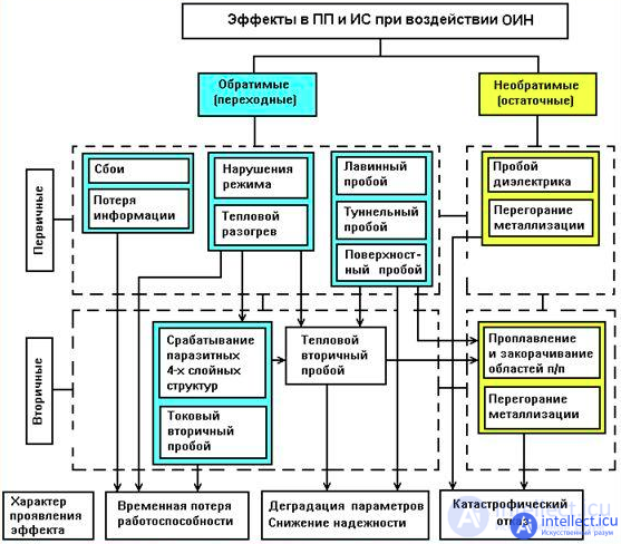
Figure classification of effects arising in semiconductors (PP) and integrated circuits (IC) when exposed
single voltage pulses (SPE)
The main effects of PP and IS damage and their relationship with SPE parameters
According to the time and nature of development, the effects are divided into primary and secondary.
- The primary effects develop due to the energy of the SPE itself during its action. The primary ones include failure and loss of information in the elements, thermal heating, breakdown of a gate insulator, avalanche and tunneling breakdown, metallization burnout under the influence of induced currents. Primary effects may not cause failure on their own (for example, a tunnel breakdown), but they may contribute to their development and transition to a secondary form.
- For the development of secondary effects, it is necessary to accumulate energy in the internal volume of the semiconductor region, for which some time is required (for example, heating the semiconductor region to the melting point in the secondary breakdown). Energy for the development of the secondary effect can be provided by the SPE itself and (or) borrowed from internal sources (power source, storage capacitors). The nature of the development of secondary effects can be regenerative and non-regenerative.
By the nature of the effect on the parameters of the elements, primary and secondary effects are divided into reversible (transient) and irreversible (residual).
- Transitional effects cause a temporary loss of operation of the PCB and IC under the influence of induced currents and voltages, which manifests itself in the form of a malfunction (false response), a change in the internal state of the element, the mode goes beyond acceptable limits, etc. In this case, after SPE exposure, the element is restored to working capacity after a time tpr - the time of loss of working capacity.
- Residual effects (damage effects) can be of a parametric nature (the exit of one or a group of parameters beyond the permissible limits) or a form of catastrophic failure.
Catastrophic failures in the devices are associated with the following parameters of electrical signals affecting the internal elements of the PP and IS, and their levels.
1) Exceeding the energy released in a certain internal element for a certain time, the limit level (level of damage):
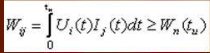
where Ui (t), Ij (t) is the current and voltage on the element under consideration; tи - signal action time; Wп (tи) is the level of damage to the internal element, depending on the duration of the acting pulse. This criterion is used to determine the resistance levels of PP and IP associated with the effects of thermal secondary breakdown of semiconductor regions. Sometimes the level of resistance to these effects is determined by the power dissipated in the element for a given time, i.e.
Both of these criteria are equal and are energy.
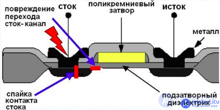
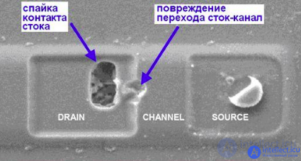
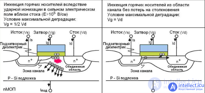
Rice Breakdown of the transition of the drain channel with the subsequent formation of adhesions in the contact area
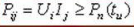
2) Exceeding the current flowing through the selected internal element, the limit level (level of damage):

where Ip is the maximum permissible current level. This criterion describes the effect of the current secondary breakdown in the PP, burnout metallization in the PP and IS.

Rice Burnout of nichrome and polysilicon metallization
3) Exceeding the voltage applied to some internal element, the limit value:

where Uп is the maximum permissible voltage level. Such a criterion is used to determine the level of resistance by the mechanisms of dielectric breakdown and, in some cases, reverse biased pn junctions.
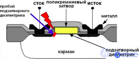

Fig Damage gate dielectric
4) Exceeding the voltage applied to the internal element of a certain threshold value while simultaneously being able to provide a threshold current value through the element:

where Uпор, Iпор - threshold values of voltage and current on the element, necessary for the development of this effect. This criterion describes the triggering (“snapping-in”) of the parasitic four-layer structures (thyristor effect) under the influence of overvoltage pulses, where Uпор = Uavl (turn-on voltage) of the structure, and Iпor = Iud (holding current).
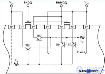

Rice The effects of a parasitic four-layer structure
5) The excess of the rate of change of voltage on some internal element of the limit value:

where (dU / dt) pr - the maximum rate of change of voltage on the element. Such a mechanism is characteristic for the inclusion of certain types of parasitic four-layer structures in CMOS ICs. For the development of the process of the thyristor effect, it is necessary that the voltage and current on the structure are greater than some holding values Uud, Iud. The similar parameters describe the resistance of PP and IS to SPE associated with the degradation of electrical parameters, but, unlike catastrophic failures, the dependences are not threshold, but continuous.
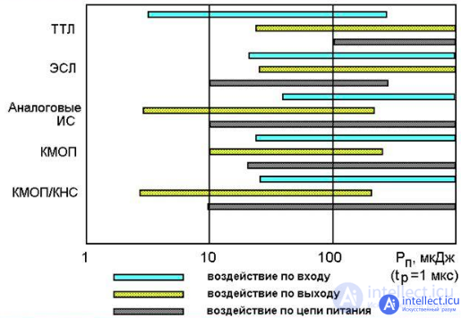
Fig Ranges of resistance levels of typical ICs to SPEs
Hidden effects of PP and IP damage
ESD (electrostatic discharges) may also cause slight damage, which nevertheless leads to device failure during operation in the initial period. Latent defects may not appear immediately after discharge, but months or years later. They can be divided into three categories: - the damage caused is so small that the device fully complies with the rating characteristics. The likelihood of a trouble-free operation over the entire service life is high; - the damaged element of the device slightly exceeds the established parameters and is quite capable of performing its functions in the system. However, there is a reasonable likelihood of premature failure; - the device is operational, but does not meet all the requirements for it. The reliability of the device is significantly weakened.According to the physical principle, latent defects are also divided into three groups.
Rice One of the possible mechanisms of parametric degradation of IP due to the influence of overvoltages

Rice Visual degradation of IP beam output
The latent effects of IP damage caused by exposure to SPEs are often difficult to identify. The device continues to function normally, electrical parameters remain normal, but its reliability decreases.
ESD protection methods
1) Application of limiters (gas-discharge, ferrite, diode limiters based on pn junction, diode limiters based on pin junction), varistors based on metal oxides, Limiters based on GaAs Schottky microwave diodes

2) the use of protective shields and protective conductive textiles with silver threads
Damage to electronic devices due to statics is difficult to detect. The fact is that static discharges can lead to significant damage, which destroy the "evidence" of the participation of statics. Electronic components are most vulnerable when they are mounted on a printed circuit board. Consider the effects of static.
Dust accumulation. Static charge attracts dust. The accumulation of dust in an unpressurized unit can lead to breakdown, for example, in high-voltage devices (TVs, monitors, etc.), where dust becomes an ideal way to spread breakdown.
Static charge generation. Static charge generation is highly dependent on the level of humidity. Voltages up to 20 kV can be generated by a person walking on a carpet if the relative humidity level is below 30%. At high humidity, the same walk will result in a lower charge of 1.5 kV. Obviously, in the absence of antistatic measures, the charge accumulated by a person can damage the device.
Sensitivity to electrostatic discharges. Even low voltages can cause breakdown of electronic components. For example, a small discharge of 30 V can destroy the gate of the MOS transistor if the thickness of the silicon oxide in the structure of the transistor is small.

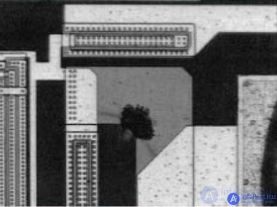
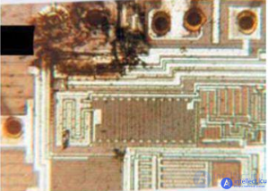
Figure: Chip crystal damage caused by electrostatic discharge
The negative effect of electrostatic discharge primarily affects the MOS and CMOS ICs. electrostatic discharge causes the following types of damage: thermal breakdown of the pn junction, the formation of voids in the oxide (Fig. 1, [3]), the melting of metal conductors, etc. Some bipolar devices are also sensitive to electrostatic discharge. Especially dangerous are electrostatic discharges for TTL ICs with a Schottky barrier, which break through at ESR energies 2–3 times lower than necessary for the breakdown of TTL ICs. This is due to the smaller Schottky barrier. The sensitivity thresholds of semiconductor devices and ICs are given in table 1, the relative sensitivity of various types of ICs to ESD is in table 2
Table 1. Sensitivity thresholds for semiconductor devices and integrated circuits
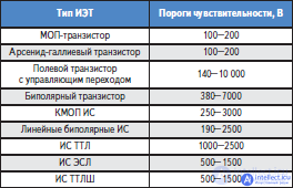
Table 2. Relative sensitivity of various types of integrated circuits to electrostatic discharges

Aging is a relatively slow change in the physicochemical properties of materials during storage and operation. All metals and insulating materials are subject to aging. Aging time depends on the degree of environmental impact and operating conditions. As a result, the aging of materials causes the corresponding aging of the elements of the equipment. So, the aging of non-wire resistors is characterized by a slow irreversible increase in resistance. The average change in resistance is 1.5 - 3% per year. The aging rate of some resistors reaches 5 - 10% per year.
Reducing the influence of aging processes on the reliability of equipment can be achieved by using high-quality materials with low aging rates; appropriate regimes determining low aging rates; correctly selected circuit solutions in which significant changes in the parameters of the elements do not lead to failures.
The impact of qualifications of staff. In the process of servicing devices, storing and transporting devices, the possibility of various errors by operating personnel (improper switching on, inaccurate adjustment, accidental shock, etc.) is not ruled out. Obviously, the number of errors will be the smaller, the higher the qualification of the maintenance staff, the better he knows the technique and the more experience he has in work. The possibility of errors increases with the complication of the situation and the deterioration of external conditions (the occurrence of several failures at the same time, severe frosts, etc.).
When carrying out maintenance activities, maintenance workers can also make mistakes related to time delays and neglected preventive and repair work, incorrect replacement of instruments, inaccurate readouts on the scale of measuring instruments, etc. All these errors can lead to immediate failures or significantly reduce operational reliability during subsequent operation of the equipment. Therefore, the paramount requirement for the maintenance staff is a careful attitude to the matter and strict technological discipline in the implementation of the established service order.
The possibility of erroneous operation in operating conditions also depends on ease of maintenance, maintainability of elements and systems.
A great influence on the proper functioning of the devices is exerted not only by the qualifications of the attendants, but also by the degree of their training in performing preventive work and eliminating failures. In this regard, the use of widely used so-called simulators should be recommended, on which artificial failures are created and then eliminated by maintenance personnel in the laboratory. It is also possible to reduce the impact of staff qualifications on operational reliability by automating the control of equipment parameters, using devices that fix the place of failure, automating the search for failures, and simplifying test equipment.
Many degradation phenomena in the active elements of microelectronics are currently associated with diffusion - the process of mass transfer in the
bulk of a semiconductor, on its surface, along phase boundaries and in contacts. It is this process, which can be accelerated depending on the
presence of dislocations, internal mechanical stresses, and such external factors as pressure, temperature, electric field, radiation, etc.,
causes the degradation of the electrical characteristics of the device, creep, aging, corrosion of materials of the semiconductor structure and contacts .
The specificity of degradation mechanisms is most clearly manifested depending on the method of creating a rectifying contact. So,
Experimental studies of Schottky barrier diodes based on gallium arsenide and silicon in various operating modes showed [14] that the
main physical process causing the degradation of parameters is interdiffusion at the metal – semiconductor – metal – metal interfaces. Mutual diffusion leads to the formation of intermetallic compounds at the metal-semiconductor interface and to the generation of deep centers
in the space charge region [15], to a deterioration of the breakdown voltage of the Schottky barrier [16-18].
For diodes with a Schottky barrier, along with the mutual diffusion of components, an important mechanism of degradation is the relaxation of internal
mechanical stresses.
The effect of plastic deformation on the characteristics of semiconductor devices is due to an inhomogeneous change in the
concentration of carriers, their lifetime, and other properties of the material of which the device is made. A correlation of excess reverse currents of
semiconductor diodes with the dislocation density in the base was noted in [16]. Generation-recombination
centers associated with dislocations , changes in the semiconductor band structure caused by the deformation field of dislocations can manifest themselves in the appearance of
tunneling currents. The authors of [19] showed that dislocations are generated very efficiently during thermal compression due
to the temperature gradient and local plastic deformation. For modern ICs with a high degree of integration, one of
The dominant failure mechanism is the process of degradation and destruction of microconductors of multilevel metallization and its elements due to
electromigration [20, 21].
Electromigration (electrodiffusion) is the mass transfer observed in metals and semiconductors when a constant and alternating
electric current of high density passes , is the main form of manifestation of ionic conductivity, as a result of which this process is called
electrotransfer. The ion transport mechanism is diffusive, for example, the diffusion of ions over the surface, grain boundaries, dislocations
(there are other transport mechanisms, such as vacancy and thermal diffusion of interstitial atoms [22]).
fall into the categories of commercial, industrial, military and space.
Часть 1 The influence of external factors on the reliability of electronic equipment and components - heat,
Часть 2 Effects of radiation on electronic components - The influence of

Подробнее о диагностике и поиске неисправностей
https://intellect.icu/testy-i-sovety-po-proverke-i-diagnostike-neispravnostej-radioelementov-diodov-tranzistorov-kondensatorov-termistorov-i-optopar-3260
Здесь больше теории о диагностике https://intellect.icu/5-neispravnosti-aktivnykh-i-passivnykh-elektroradioelementov-rezistorov-diodov-tranzistorov-kondensatorov-i-mikroskhem-3304
склейка линз была так называемым канадским бальзамом - смолой канадской пихты
Comments
To leave a comment
Diagnostics, maintenance and repair of electronic and radio equipment
Terms: Diagnostics, maintenance and repair of electronic and radio equipment