Lecture
The sequential conversion of binary information requires the organization of storing the initial data, intermediate and final results on the storage elements. Temporary data storage is necessary to wait for arguments that arrive at different times, for multiple data transfer to different devices, etc.
Most modern digital devices are sequential or digital automata with memory, consisting of combinational circuitry and memory elements - storage elements (GE) (Fig. 4.1).
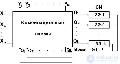
Fig. 4.1. Generalized memory circuit structure
Elements for storing binary information should have three modes of operation: recording, storing and issuing information.
In storage mode, GEs are in one of two states: zero or one. In recording mode, it is possible to record “0” or “1”. The mode of issuance is usually not organized. As a rule, GE have two permanent exits: direct (  - output), showing the state of the GE, and inverse (
  -out) equal to the inversion of the signal on the direct output.
The presence of memory in the circuit allows you to memorize intermediate processing states and take their values into account in further transformations. The output signals Y = (Y 1 , Y 2 , ..., Y m ) in the circuits of this type are formed not only by the set of input signals X = (X 1, X 2 , ..., X n ), but also from the states of the memory circuits. In this case, the current discrete moment of time t and the subsequent (t + 1) moment of time are distinguished.
(Fig. 4.1).
The transfer of the Q value between the moments of time t and (t + 1) is carried out with the help of synchronizing pulses (SI).
The simplest numeric elements include the trigger, registers, counters, and level distributors.
Triggers are elementary automata containing the actual memory element (EP) or latch and control circuit. The latch is built on two inverters connected with each other "crosswise", i.e. so that the output of one is connected to the input of the other (Fig. 4.2).
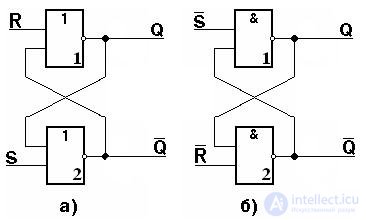
Fig. 4.2. Bistable cells on LE OR NOT (a) and AND NOT (b)
Such a connection gives a circuit with two stable states (therefore, an EP is also called a bistable cell (BS) , that is, with two stable states). Indeed, if the output of the inverter 1 has a logical zero, then it provides at the output of the inverter 2 a logical unit, due to which it itself exists. The same signal matching also takes place for the second state, when inverter 1 is at “1” and inverter 2 is at “0”. Either of the two states can exist indefinitely, provided there is a supply voltage and no external control signals.
The state of the trigger is recognized by its output signal. Under the influence of the input signal, the trigger can jump from one steady state to another, while the voltage level of its output signal changes abruptly. The transition to each subsequent state usually depends not only on the current values of the input signals, but also on the previous state of the trigger. Information about the previous state, coming from the outputs along with external signals, controls its operation. Therefore, triggers are feedback devices.
Triggers in computing device designs usually have two outputs: direct and inverse . In a single state at the exit high signal level, and in the bullet - low. At the exit - vice versa.
Trigger schemes can be divided into several types: with setup inputs - RS - trigger, with counting input - T-trigger, as well as D-, JK-triggers, etc.
If at least one input information is forcibly entered under the influence of a synchronizing signal, then the trigger is called synchronized (synchronous). If the entry of information on any input is made without a synchronizing signal, the trigger is called non-synchronized (asynchronous).
The laws of the functioning of the triggers are given in transition tables.
Triggers can be classified according to various criteria. Figure 4.3 gives a classification of triggers according to three major characteristics: the logic of operation, the method of recording information, and the type of storage element.
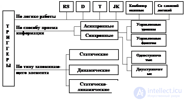
Fig. 4.3. Classification of triggers used in digital circuitry
As mentioned earlier, an asynchronous trigger is a device, the entry of information on any input of which is made without a synchronizing signal. This means that the state of the outputs of such triggers depends only on the combination of input (information) signals and their current state.
Depending on the type of logic elements, on the basis of which bistable cells (BL) of triggers are built, there are distinguished triggers with direct and inverse input logic. In fig. 4.4, and the graphic designation RS of a trigger with direct input logic, the BL of which is built on OR-NOT elements (see Fig. 4.2, a), is presented. In fig. 4.4, b and 4.2, b are presented, respectively, the graphic designation of the RS trigger with inverse inputs and BL on the elements of NAND, on the basis of which it is built.
The operation of this trigger is described in table. 4.1.
Table 4.1
| R | S | Q t | Q t + 1 | Stages in the timeline | Note | |
| 0.6 | R = 0; S = 0 | Data storage | ||||
| 2.4 | ||||||
| Set | Set to 1 | |||||
| Reset | Set to 0 | |||||
| X | R = 1; S = 1 | Forbidden combination | ||||
| X |
Functions of RS trigger outputs (characteristic equations):
 (4.1)
(4.1)
 . (4.2)
There are various types of functioning RS trigger, get acquainted with them:
The conditional graphic designation of this trigger is presented in fig. 9.4, and time diagrams of his work - in Fig. 9.5.
Fig. 4.4. Conditional graphic designation of asynchronous RS trigger with direct (a) and inverse inputs (b)

Fig. 4.5. Timing diagrams of the asynchronous RS trigger with direct inputs
The time diagrams show the various stages of the state in time of the input and output signals of the asynchronous RS trigger in accordance with Table 4.1, while the initial state of the trigger at the time t = 0 corresponds to "0".
There are modifications of RS triggers on the basis of their reaction to a forbidden ( R = 1 and S = 1 ) combination of control signals. According to this feature, such triggers can be:
R-flip-flops , different from RS flip-flop in that if there is a forbidden combination at the input, it is set to "0". The symbol of this trigger and the table of its work are presented, respectively, in fig. 4.6, a and 4.6, b.
S-flip-flop , which differs from RS flip-flop in that if there is a forbidden combination at the input, it is set to "1". The symbol of this trigger and the table of its work are presented, respectively, in fig. 4.7, and 4.7, b.
An E-trigger that differs from an RS trigger in that if there is a forbidden combination at the input, this trigger retains its previous state. The symbol of this trigger and the table of its work are presented, respectively, in fig. 4.8, and 4.8, b
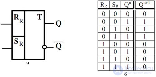
Fig. 4.6. Graphic designation of the R-flip-flop (a) and table of its work (b)
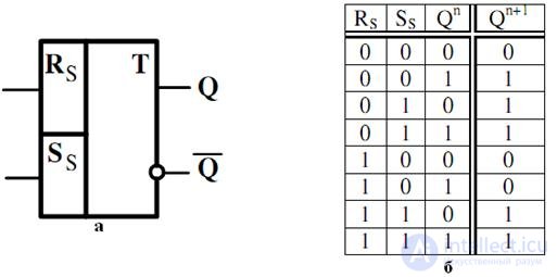
Fig. 4.7. Graphic designation of S-trigger (a) and a table of its work (b)
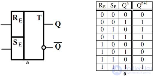
Fig. 4.8. Graphic designation of the E-trigger (a) and the table of its work (b)
DV trigger
D-trigger
Trigger type D ( from English Delay - delay) has one input. Its state on the direct output repeats the input signal, but with a delay determined by the clock signal arriving at the synchronous input. On this basis, it follows that the asynchronous D-trigger has no practical application. However, in order to further develop the theory of trigger devices, we present the graphical designation of the D-trigger (Fig. 4.9, a) and its table of work (Fig. 4.9, b).

Fig. 4.9. Graphic designation of D-flip-flop (a) and table of its work (b)
The characteristic equation of the direct and inverse outputs of the D-flip-flop, compiled on the basis of the transition table, have the form:
 (4.3)
(4.3)
 . (4.4)
The DV trigger differs from the D trigger in that, due to the control signal V, it is possible to avoid the drawback inherent in the asynchronous D trigger. Namely: if the input is V = 0 , then the DV- trigger stores information (see the table in Fig. 4.10, b), and when V = 1 , it works as D - the trigger. In fig. 4.10, and the graphical designation of the DV trigger is presented, and expressions (4.5) and (4.6) describe the functions of the forward and inverse outputs of this trigger.
 (4.5)
(4.5)
 . (4.6)

Fig. 4.10. Graphic notation DV-trigger (a), a table of his work (b)
Before getting acquainted with this trigger, it is necessary to note the fundamental difference between a trigger of this type, as well as a trigger of JK type (to be discussed later), from the previously considered types of triggers. The difference is that RS- and D-flip-flops have an open- ended structure (we are not talking about internal feedbacks in the BL circuit now), and the T- and JK- type flip-flops use output signals to influence their inputs.
A T- trigger is a device that changes its state to the opposite when the active signal level arrives at its input. Those. when a trigger of a series of signals consisting of “0” and “1” arrives at the input, each second “1” at the output will have “0” at the direct output of the trigger, provided that its initial state is zero. It turns out that the T-trigger counts “1” at its input and, if an even number “1” (or “0” at the inverse input) arrived at the input, its output will be “0”, otherwise - “1”. Because of this, the T input of this trigger is called countable . The table of operation of this trigger is presented in Fig. 4.11, b, graphic designation - in fig. 4.11, a. The characteristic equations of its direct and inverse outputs have, respectively, the form (4.7) and (4.8).
 (4.7)
(4.7)
 . (4.8)

Fig. 4.11. T-flip-flop graphic (a), table of its work (b)
JK - the trigger differs from the RS - trigger in that if there is a forbidden combination at its input , the states of the outputs of the JK - trigger are inverted . To do this, as well as the T-trigger JK - trigger uses its outputs to influence its inputs.
The graphic designation of this trigger is shown in fig. 4.12, and, the table of work - on fig. 4.12, b. The characteristic equations of its direct and inverse outputs have, respectively, the form (4.9) and (4.10).
 (4.9)
(4.9)
 . (4.10)
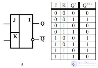
Fig. 4.12. Graphic notation JK-trigger (a), a table of his work (b)
Unlike non-clocked triggers, the transition to a new state in synchronous (clocked) triggers with a special input occurs only when the clock signals are applied to this input. Clock signals are also called synchronization , executive , command , etc. and are denoted by the letter C (from the word Clock - the clock, in this case means “time control”).
By way of the perception of clock signals, the triggers are divided into level controlled and front driven .
Level control means that with one level of the clock signal, the trigger accepts input signals and reacts to them, while with the other, it does not perceive and remains in an unchanged state.
When the front is controlled, switching permission is given only at the time of a drop in the clock signal (on its front or in a fall). At other times, regardless of the level of the clock signal, the trigger does not perceive the input signals and remains unchanged. Triggers controlled by the front are also called dynamically controlled triggers.
In addition to dividing synchronous triggers according to the method of perceiving clock signals, triggers are also divided according to the nature of the switching process: one -step and two-step . In a single-stage trigger, switching to a new state occurs immediately, in a two-stage one, in stages.
In fig. 4.13 shows the processes occurring in synchronous triggers. The clock pulse diagrams show the content of the processes at individual stages of trigger switching, and below the diagrams the synchronization input for various types of synchronization is given.
Fig. 4.13 Processes occurring in synchronous triggers
As an example of the functioning of synchronous triggers consider the operation of the synchronous RS-flip-flop. The operation of this trigger is described in table 4.2.
Table 4.2
| WITH | R | S | Q t | Q t + 1 | WITH | R | S | Q t | Q t + 1 |
| X | |||||||||
| X |
Comparing tables 4.1 and 4.2 of the work, respectively, asynchronous and synchronous RS-flip-flop, it is clear that the second differs from the first one in that the input synchronization signal C appears in it.
As we see, the first eight combinations of input signals of the synchronous trigger correspond to the value C = 0 , at which no combination of signals R and S leads to a change in its state. When C = 1, the work of the synchronous RS-flip-flop repeats the work of the asynchronous one . It follows from this that if in the characteristic equation the arguments R a and S a are replaced, respectively, by the functions R a = RC and Sa a = SC , where Ra and Sa are the asynchronous input signals and R, S and C are the input signals synchronous RS-trigger, then the characteristic equation for asynchronous and synchronous triggers will be the same.
If the BL, based on the asynchronous RS trigger, is built on LE OR NOT, then the functions R a and S a for the synchronous trigger in the same basis take the form:  and
and  .
.
The form of the same functions, but in the NAND basis, taking into account the inverse input signals of the BL (see Fig. 4.2, b) is as follows:  and
and  .
.
In fig. Figure 4.14 shows the functional diagrams of the synchronous RS-flip-flop in the basis of the OR-NOT (a) and N-NOT (b).
Fig. 4.14. Functional diagram of the synchronous RS-flip-flop in the basis of the OR-NOT (a) and AND-NOT (b)
Synchronous RS trigger with front sync
RS trigger with level sync
In fig. Figure 4.15 presents a graphic designation of an RS flip-flop with level synchronization with direct inputs. To change the information in such a trigger d. active (“1”), in addition to the signal at one of the information inputs, is also a signal at the sync input (see. Fig. 4.15, b).
As can be seen from the presented time diagrams of this trigger operation, the moment of its switching (transition from one state to another) is determined by the moment of appearance of the unit level signal at one of the information inputs , provided that there is a “1” at the sync input, or the moment when “1” is set to synchronization input , provided the presence of "1" on one of the information inputs . This is true for positive logic triggers with any logic for working with level synchronization.
Fig. 4.15. Graphic designation of the synchronous trigger (a) and time diagrams of its work (b)
Unlike a synchronous trigger with level synchronization, the moment of trigger switching with front synchronization is determined by the moment the signal is switched on the sync input , provided that there is an active level at one of its control inputs. If at the time of action of the active for this type of front trigger, there is no active signal level on its control inputs, then the trigger will remain in storage mode.

Fig. 4.16. Graphic designation of the synchronous RS trigger with synchronization on the front (a) and rear (b) front and timing diagrams of their work, respectively, (c) and (d).
Taking into account the fact that there are two moments of switching the clock signal: the transition from state “0” to state “1” and from state “1” to state “0” , there are two types of such triggers. In fig. Fig. 4.16, and the graphic designation of the synchronous RS trigger with synchronization along the leading edge (from “0” to “1”) and timing diagrams of its operation at the moment of switching (Fig. 4.16, c) are presented. In fig. 4.16, b and 4.16, g are presented, respectively, the graphic designation of the synchronous RS trigger with synchronization on the falling edge (from “1” to “0”) and timing diagrams of its operation.
The considered trigger devices belonging to the class of single-stage triggers contain only one BL. Как только на входе одноступенчатого триггера изменяется установочная комбинация, на выходах немедленно (без учета переходных процессов) изменяются выходные уровни, свидетельствующие об изменении состояния триггера. Подобная реакция в ряде случаев недопустима. В общем случае она не позволяет управлять выработкой новых значений установочных входов собственным действующим состоянием, а также состояниями всех других переключаемых в том же такте триггеров. В частности, одноступенчатые триггеры нельзя непосредственно использовать в сдвигающих регистрах, в одноразрядных пересчетных схемах по модулю 2 и т.д.
In all such schemes, two-stage triggers containing at least two BL are used. Such triggers are called MS triggers (Master – Slave - master-slave). Both triggers function as synchronous triggers with static control (Fig. 4.17).

Fig.4.17. Functional two-stage trigger scheme
If the sync input C = 1, the leading trigger is set to the state corresponding to the signals received at the information inputs. The slave trigger, which has an inverse clock input, while not immune to the information received at its input from the output of the leading trigger. It continues to be in the state in which it was previously installed (in the previous clock period). When changing the value of C(from “1” to “0”) the leading trigger is disconnected from the information inputs and stops responding to changes in the signals at these inputs; the slave trigger is set to the state in which the master trigger is located. From this point on, the outputs are set to the values corresponding to the input signals arriving at the time of the considered signal edge at the clock input.
Thus, the process control in the trigger with two-step information storage during the clock period is carried out by two fronts of the signal at the synchronization input: the leading trigger is set at the positive front, the slave is set at the negative front.
MS-triggers are based on two-step synchronous RS-, JK-triggers and others. Below are two-step triggers based on the listed triggers.
Synchronous push-pull RS-trigger . Stable operation of a single-cycle RS flip-flop in an arbitrary scheme is possible only under the condition that information is entered into a trigger after the transfer of information about its previous state to another trigger is completed. For this, it is necessary to use two series of out-of-phase clock pulses. This principle of information exchange is implemented in two-stroke RS-triggers (Fig. 4.18).
 |
Fig.4.18. Functional diagram of the push-pull RS-trigger on the elements and HE (a) and its conventional graphic designation (b)
When a pulse C = 1 arrives at the input, the input information is recorded only in the first single-cycle RS trigger, while the second trigger will store information related to the previous presentation period. At the end of the synchronization pulse (  = 0,
= 0,  = 1), the first RS-flip-flop will go into storage mode, and the second will overwrite the new output signal from it. The push-pull trigger will change its state only after the termination of the synchronization pulse (switching to the information storage mode). To set the trigger to the state 0 or 1 without the use of sync pulses, additional inputs were introduced into the circuit.
 and
and  non-synchronized installation.
In practical digital circuitry, sometimes there are situations when there is a need to design triggers with the required logic of operation based on the available triggers.
To solve this problem, there are the following methods for designing triggers:
- design method using RS-flip-flop,
- method of transformation of the characteristic equation,
- method of comparison of characteristic equations.
Designing triggers based on RS-trigger
Consider this method on the example of designing RS-flip-flop modifications: R-flip-flop. When designing triggers based on RS flip-flops, it is necessary to design a control circuit for its inputs.
Для R триггера : R R и S R – входы схемы управления, R и S – выходы схемы управления и входы RS-триггера. По определению, R-триггер при наличии запрещенной комбинации должен установиться в «0», а для RS-триггера – это режим установки в «0» (R=1, S=0). Исходя из этого следует, что функции выходов разрабатываемой схемы управления RS-триггером (см. рис. 4.19,а) будут иметь вид (10.1)
 . (4.11)

Fig. 4.19. Исходная схема для проектирования R-триггера и функциональная схема R-триггера в произвольном базисе (б)
Суть данного метода поясним в процессе проектирования JK-триггера на основе RS-триггера .
Сравним выражения (4.1) и (4.9), описывающие функции прямых выходов, соответственно RS- и JK-триггеров, а также (4.2) и (4.10), описывающие функции инверсных выходов, соответственно RS- и JK-триггеров. В результате сравнения получим, что
 and
and  . (4.12)
Подставив в (4.1) и (4.2) вместо аргументов R и S , значения функций (4.12) и выполнив необходимые преобразования, получаем в результате:
 (4.13)
  (4.14)
Доказательства (4.13) и (4.14) подтверждают справедливость (4.12), а это значит являются функциями выходных сигналов схемы управления RS-триггера, позволяющими на его основе реализовать функции JK-триггера.
Функциональная схема спроектированного JK-триггера представлена на рис. 4.20.
Fig. 4.20. Функциональная схема JK-триггера на базе RS-триггера на логических элементах И
Функциональные схемы двух триггеров (R- и JK-), построенных на базе одного и того же RS-триггера, позволяют наглядно продемонстрировать понятия разомкнутой и замкнутой структуры триггеров, о которых упоминалось ранее. In fig. 4.19 отсутствуют обратные связи с выходов RS-триггера на вход схемы управления этим триггером, что и является признаком того, что структура R-триггера является разомкнутой . From fig. 4.20 видно, что на схему управления RS-триггера – основы для проектирования JK-триггера поступают помимо входных сигналов J и K поступают сигналы  and
and  RS-триггера, что является признаком замкнутой структуры JK-триггера.
Т-триггер
Метод сравнения характеристических уравнений
Существуют универсальные триггеры, на базе которых можно проектировать другие триггера. К таким триггерам относятся JK - и DV -триггеры
Для пояснения данного метода рассмотрим процесс проектирования RS -триггера на базе JK -триггера.
Сравнивая характеристические уравнения этих триггеров, можно сделать вывод о том, что на базе JK-триггера можно построить RS-триггер, если обеспечить условие JK=0 . Реализовать это условие для асинхронных триггеров не представляется возможным, т.к. не представляется возможным описать функции выходов J и K схемы управления базового JK-триггера, определяемые ее аргументами R и S . Однако, если в качестве базового триггера взять синхронный JK-триггер, то с помощью функций: K = R , J = S и  , где K , J и С * – информационные входы и синхронизации базового JK-триггера, а R , S и С - информационные входы и синхронизации проектируемого RS–триггера, мы достигаем поставленной цели. Функциональная схема спроектированного по данному методу RS–триггера на базе JK-триггера представлена на рис. 4.21.
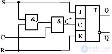
Fig. 4.21. Функциональная схема RS–триггера на базе JK-триггера
Схемы синхронных RS- и JK-триггеров составляют основу для получения других триггерных схем. In fig. 4.22÷4.24 представлены различные схемные решения триггеров, построенных на их основе.
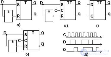
Fig. 4.22. Т-триггер: (а) – несинхронизируемый, (б) - его временная диаграмма, (в) – синхронизируемый и (г), (д) – соответственно, условное графическое обозначение и его временная диаграмма
Простейшая схема несинхронизируемого Т-триггера представлена на рис. 4.22,а. При Т=1 для двухступенчатого триггера сигнал на его выходе изменится только по завершению действия Т=1, что способствует возникновению генерации в схеме с обратной связью. Можно считать, что в данной схеме единичный входной сигнал представляется спадом сигнала Т=1, так как при любой продолжительности сигнала Т=1 изменение состояния Т-триггера происходит только 1 раз – при снятии сигнала Т=1 (рис. 4.22,б).
Для представления потенциалом последовательности единиц на входе Т-триггера используется синхронизируемая схема (рис. 4.22,в, г). Здесь единичный входной сигнал представляется высоким уровнем сигнала Т при С=1. Поэтому высоким уровнем сигнала Т можно представить последовательность 1 (рис. 4.22,д). Запись в триггер происходит при С=1, причем смена состояния происходит после окончания действия сигнала синхронизации С=1. При Т=1 состояние триггера изменяется на противоположное, а при Т=0 не меняется.
Наиболее широко используемый, реализует функцию временной задержки. Предназначен для хранения состояний (1 или 0) на один период тактовых импульсов (задержка на один такт). Имеет режимы установки 1 или 0. В связи с этим несинхронизируемый D-триггер (рис. 4.23,а) не применяется, т.к. на его выходе будет просто повторяться входной сигнал. Синхронизируемый однотактный D-триггер (рис. 4.23,б) задерживает распределение входного сигнала на время паузы между синхросигналами (задержка на полупериод). D (Delay – задержка) – вход установки в единичное или нулевое состояние на время, равное одному такту.
 |
При С=1 триггер устанавливается в состояние, определяемое логическим уровнем на входе D (при С=0 он сохраняет ранее установленное состояние  ). Такое функционирование может быть описано логическим выражением:
  . D-триггер можно спроектировать на базе любых RS- или JK-триггеров, если на их входы одновременно подать взаимно инверсные сигналы.
Fig. 4.23. D-триггер: (а) – несинхронизируемый; (б) – синхронизируемый однотактный; (в) – двухтактный и его условное графическое обозначение (г); (д) – временная диаграмма работы двухтактного D-триггера
In fig. 4.24 представлены варианты построения различных триггеров на базе синхронного JK-триггера.
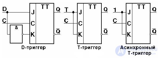
Fig. 4.24. Способы использования JK-триггера
Регистр – последовательностное логическое устройство, осуществляющее приём и запоминание n - разрядного слова (кода), х 1 , х 2 ,… х n-1 , x n , а также выполнение определённых микроопераций над этим словом. Число разрядов в регистре называют его длиной. В n -разрядном регистре может быть записано 2 n различных n -разрядных двоичных чисел, т.е. находится в 2 n различных состояниях. Регистр представляет собой упорядоченную совокупность триггеров (RS-, D- или JK- типов с динамическим или статическим управлением). Разрядность регистра соответствует количеству используемых в нём триггеров. Каждый триггер имеет прямой и инверсный выходы, используемые соответственно для получения прямого и инверсного кодов. Кроме триггеров в состав регистра входит комбинационная схема, формирующая функцию возбуждения (входные сигналы) триггеров. Регистры – самые распространенные узлы цифровых устройств. Они оперируют с множеством связанных переменных, составляющих слово. Над словами выполняется ряд операций: прием, хранение, сдвиг в разрядной сетке. С помощью регистров можно осуществлять операции преобразования информации из одного вида в другой (последовательного кода слова в параллельный и т.п.), а также некоторые логические операции (поразрядное логическое сложение и умножение и т.п.).
По виду выполняемых операций над словами различают регистры накопительные (памяти, хранения), предназначенные для приёма и передачи информации, и сдвигающие .
По количеству входных каналов регистры бывают одно- и парофазными . В однофазных регистрах информация поступает на каждый разряд только по одному каналу (прямому или инверсному), а в парофазных – по обоим каналам.
По количеству тактов управления, необходимых для записи кода слова, различают одно- , двух- и многотактные (n-тактные) регистры.
По способу приёма и передачи информации различают последовательные (с записью кода числа путем его последовательного сдвига тактирующими сигналами, начиная с младшего или старшего разряда), параллельные (с записью числа во все разряды одновременно параллельным кодом) и параллельно- последовательные регистры.
В параллельных регистрах прием и выдача слов производится по всем разрядам одновременно. В них хранятся слова, которые могут быть подвергнуты поразрядным логическим преобразованиям.
В последовательных регистрах слова принимаются и выдаются разряд за разрядом. Их называют сдвигающими, т.к. тактирующие сигналы при вводе и выводе слов перемещают их в разрядной сетке. Сдвигающий регистр может быть нереверсивным (с однонаправленным сдвигом) или реверсивным (с возможностью сдвига в обоих направлениях).
Последовательно-параллельные регистры имеют входы-выходы одновременно последовательного и параллельного типа. Существует несколько вариантов последовательно-параллельных регистров: с последовательным входом и параллельным выходом (SIPO, Serial Input – Parallel Output), параллельным входом и последовательным выходом (PISO, Parallel Input – Serial Output), а также варианты с возможностью любого сочетания способов приема и передачи слов.
Для современной схемотехники характерно построение регистров на триггерах, преимущественно с динамическим управлением. Многие регистры имеют выходы с третьим состоянием, некоторые из них относятся к числу буферных, т.е. рассчитаны на работу с большими емкостными и/или низкоомными активными нагрузками. Это обеспечивает их работу непосредственно на магистраль без дополнительных схем интерфейса.
The purpose of memory registers is to store a small amount of binary information for a short period of time. Registers are a set of synchronous triggers, each of which stores one digit of a binary number. Input (recording) and output (reading) of information is produced by a parallel code. Input is provided by a clock pulse (with the arrival of the next clock pulse, the recorded information is updated). Reading is performed in direct or reverse code.
In fig. 4.25 is a diagram of the push-pull register based on RS triggers. Information is entered in the register on the tires x 1 , x 2 , ... x n , only in the case when the control signal of information reception is sent to the bus P p .
In this case, the signals for setting the triggers to state 1 pass through the & 1 circuit only in those bits where x 1 = 1. In order for the remaining digits to be written 0, you must first set all digits to the zero state. The word code recorded in the register will be stored in it until the installation signal is set to state 0. The direct code stored in the register of the word will be issued if there is a control signal “Issuing a direct code” on the bus В п . At the same time, the code of the word from the direct outputs of the register trigger passes through the group of circuits & 2 and in each digit the output will be generated  .
.
The “Issue of an inverse code” signal B also allows to receive the inverse code value stored in the register through the & 3 group of schemes. At the same time in each of its discharge code value is generated.  .
.
Fig. 4.25. Functional two-register register on RS-triggers
From the static registers (memory registers) are compiled register register blocks - register files . Such blocks allow independent and simultaneous recording of one word and reading of another.
For example, the IR26 chip from the KR1533 or K555 series allows you to store 4 four-digit words. The information inputs of the registers RG1 ÷ RG4 are connected in parallel (see fig. 4.26). The WA and WB entry address entries give 4 combinations, each of which allows the corresponding register to receive information from the data inputs D 1-4 , provided there is a write permission on the input  active low signal. With a high input signal Data and address entries are not allowed. The output is given from the register file in the direct code.
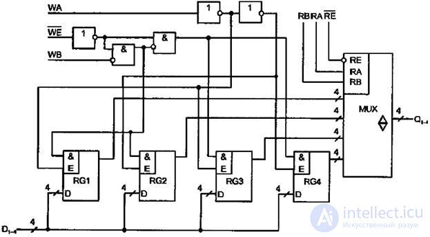
Fig. 4.26. Register File Scheme
The contents of the file (the output of one of the registers RG1 ÷ RG4) is called on the output of the Q 1-4 block using a read decoder (address inputs of the multiplexer) with the addresses RA and RB with the presence of a low active read enable signal  . With a high signal level the outputs of Q 1-4 are in a high impedance state.
They are intended to perform a bitwise shift operation of the stored binary word information after each clock pulse (by signal C) , that is, to move all digits of the word in the direction from the highest to the least significant digits (right shift) or from the lower to the highest digits (left shift). A reverse shift register can shift information both to the left and to the right. Shifting the code to the left by one digit corresponds to multiplying the code of a number by the base of the number system, and shifting to the right corresponds to division. This is due to the fact that the weight of each digit of the code for a positional number system is determined by its position in the code. In the register, the shift of the number on k discharges is carried out by k cycles or by k micro shift operations. The shift register contains the same transmission schemes for the inputs, as well as the registers for receiving and transmitting information, but the triggers must be double MS type (see Fig. 4.27). If you use simple triggers, such as RS, then you need to use another additional register for intermediate memorization of the word during the shift process, i.e. each register bit will consist of two triggers (Fig. 4.28).
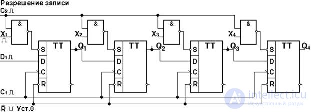
Fig. 4.27. Functional diagram of the n-bit register on D - triggers
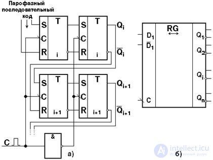
Fig. 4.28. Functional diagram of two digits of the shift register on RS - triggers (a) and conditional graphic designation of the register (b)
A shift register can be used not only to shift a code, but also to convert a parallel code received into a register into a serial one. To do this, it is enough to move the adopted code until the whole code is moved out of the register. This register can also perform the function of converting sequential code to parallel. In terms of reducing the number of connections and equipment, it is advisable to build registers on D - triggers (Fig. 4.27). Setting the register to the state "0" is performed by a negative pulse applied to the input. . The parallel code is fed to the inputs X 1 ÷ X 4 . The recording of the parallel code is carried out by a positive pulse applied to the C 2 input. The serial code is fed to the input D 1 and is recorded in the first stage of the trigger with the output Q 1 on the positive edge of the synchronization signal C 1 . In the first stages of triggers with outputs Q 2-4 on the same front, the outputs of the second stages of triggers with outputs Q 1-3 are copied. On the falling edge of the C 1 signal, the information from the first stages of the Q 1-4 triggers is rewritten to their second stages.
In the series of integrated circuits and libraries of the LSI / VLSI programmable logic, there are many variants of registers (there are about 30 of them in the TTLS circuit design). Among them are multi-mode (multifunctional) or universal, capable of performing a set of micro-operations. Multimode is achieved by composition in the same scheme of parts necessary for performing various operations. Control signals that define the type of operation being performed activate the parts of the circuit required for this.
A typical representative of multimode registers is an IC13 KR1533 chip (see Fig. 4.29). This is an eight-bit register with the possibility of two-way shifts. The register also has parallel inputs and outputs (DSR - Data Serial Right, DSL - Data Serial Left), asynchronous reset input and inputs of mode selection S 0 and S 1 , specifying four modes (parallel loading, two shifts and storage).
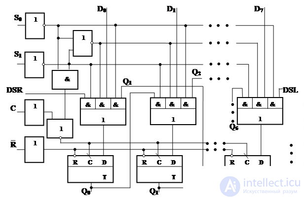
Fig. 4.29. Functional multimode register scheme
The functioning of the register is determined by table 4.2. The table applies the following abbreviations of the inputs and outputs:
X is an indifferent state, L is a low level (log. "0"),
 H - high level (log. "1"), - positive front.
Table 4.2
 Mode Mode |
Inputs | Outputs | |||||||||||||
| C | R | S 0 | S 1 | DSR | DSL | D n | Q 0 | Q 1 | Q 2 | Q 3 | Q 4 | Q 5 | Q 6 | Q 7 | |
| Reset | X | L | X | X | X | X | X | L | L | L | L | L | L | L | L |
 Storage Storage |
H | L | L | X | X | X | Q 0 | Q 1 | Q 2 | Q 3 | Q 4 | Q 5 | Q 6 | Q 7 | |
 Shift left Shift left |
HH | HH | Ll | Xx | Lh | Xx | Q 1 Q 1 | Q 2 Q 2 | Q 3 Q 3 | Q 4 Q 4 | Q 5 Q 5 | Q 6 Q 6 | Q 7 Q 7 | Lh | |
 Right shift Right shift |
HH | Ll | HH | Lh | Xx | Xx | Lh | Q 0 Q 0 | Q 1 Q 1 | Q 2 Q 2 | Q 3 Q 3 | Q 4 Q 4 | Q 5 Q 5 | Q 6 Q 6 | |
 Parallel download Parallel download |
H | H | H | X | X | D n | D 0 | D 1 | D 2 | D 3 | D 4 | D 5 | D 6 | D 7 |
Counters are sequential digital devices designed to count the number of input signals, fixing this number as a multi-bit binary number stored in triggers. They provide the conversion of a pulse code code to binary or binary decimal codes. The number of bits of the counter is determined in each case. There are one input and n outputs depending on the number of digits. In the general case, the counter has K m = 2 n (n = log 2 M) stable states, including zero. Under the action of the input signals, a counter set to a certain state saves it until the next signal arrives at the input. Each state of the counter corresponds to the sequence number 0, 1, 2,. . ., By sc. - 1 . If at time t the counter is in the ith state, then it determines the number of signals received at the counter. When applying to the input of the counter K sch . - the first input signal at its output overflow signal appears and the counter returns to the initial state, i.e. the counting of single signals is carried out in it modulo K sch . or with a period of account T = K cq . A counter-specific operation is to change their contents by one (maybe conditional).
Counters are used for the formation of addresses, commands, counting the number of cycles of operations, code generation in analog-digital converters, etc.
By way of encoding internal states, binary counters, Johnson counters, counters with the code “1 of N”, etc. are distinguished.
In the direction of the account, the counters are divided into simple (summing or subtracting) and reversible (with a change in the direction of the account). Signals arrive at simple counters with one sign, i.e. these counters have transitions from state to state in only one direction. The summing counter is designed to perform the counting in the forward direction, i.e. to add input signals (from code i to code i + 1). With the filing of the input of the next single signal counter reading is increased by one. The subtractive counter is designed to perform the counting of single signals in the subtraction mode. Each signal arriving at the input of such a counter reduces its indication by one. Reversible counters are designed to work in addition mode and subtraction mode.
By the way of organizing the account, the counters are divided into asynchronous and synchronous . In asynchronous counters, the signal from discharge to discharge is transmitted in a natural way at various time intervals, depending on the combination of input signals. Triggers do not fire at the same time. In synchronous counters, the signals from discharge to discharge are transmitted by force using clock signals. All triggers switch almost simultaneously under the action of a common clock signal.
According to the method of organizing the transfer chains between discharges, there are counters with serial , parallel and partially parallel transfer (only in groups of discharges).
The main characteristics of the meter are the counting module (counting period or conversion factor), resolution, registration time and capacity. The counting module describes the number of stable states of the counter, i.e. the maximum number of input signals that the counter can count. Resolution - the minimum permissible period of the input signals, which ensures reliable operation of the counter. The greater the frequency of receipt of counting signals, the greater the speed required from the counter. Registration time - the time interval between the moments of the input signal and the end of the longest transient process in the counter. The capacity of the counter is the maximum number of single signals that can be recorded on the counter. This counter characteristic depends on the base of the number system and the number of digits.
As with any automaton, the counter can be built on triggers of any type, but the most convenient way to do this is to use T (counting) or JK triggers, which have a counting mode for J = 1 and K = 1.
The simplest counter can be considered T - trigger. He counts up to two. The basis for the construction of counters are asynchronous or synchronous T - triggers implemented on D - triggers with dynamic control or on JK - triggers. The property of T - trigger is used to change its state when the next signal is applied to the counting input T.
Figure 4.30 shows a diagram of three digits of a summing counter built on T - triggers. The logic of his work is presented in the transition table (Table 4.3).
Table 4.3
| Entry X | condition | Mode | |||||||
| Storage | |||||||||
| Score |
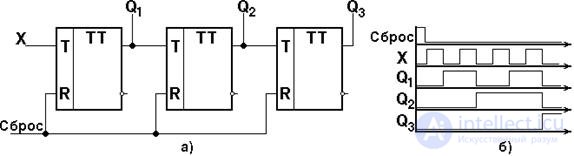
Fig. 4.30 Scheme of the functional counter on T - triggers (a) and its timing diagram (b).
In these counters, each subsequent trigger of the (i + 1) -th digit starts from the information outputs (  ,
,  ) the previous trigger of the i –th digit, and the counting signal is fed to the input of the trigger of the first digit.
A diagram of a non-synchronized binary four-digit summing counter on triggers with sequential signal transfer is shown in Fig. 4.31а, the time diagram of his work - on ris.4.31b.
Table 4.4
| X sc. | Q 4 | Q 3 | Q 2 | Q 1 | X sc. | Q 4 | Q 3 | Q 2 | Q 1 | |
Table 4.4 shows the status of the trigger trigger when exposed to a series of input signals X cf. supplied to the counting input of the first discharge.
Consider the operation of the counter, assuming that, in the initial state, it contains the code 0000. In the counter, the output of each previous trigger Q t -1 is connected to the synchronization input C t of the subsequent trigger. Signals 1 are applied to the inputs J and K of the flip-flops. The first input signal X cf. sets the trigger T1 of the counter to state 1, the remaining trigger triggers remain in state 0. The second input signal sets the trigger T1 to state 0; the third is again in state 1, etc. The input signals of the trigger T2 will be the signals taken from the direct output of the trigger T1. Thus, for the first time in state 1, the T2 trigger is established only after the first signal passes the output of the T1 trigger, and in state 0, after the second signal passes, and so on. The input signals of the T3 trigger will already be the signals taken from the direct output of the T2 trigger, etc. After a series of signals (pulses) are sent to the counter input, for example, five input pulses pass, the code 0101 (i.e. 5) is set at the output of the meter triggers, i.e. the counter counts the number of pulses applied to its input.
Typically, the meter has a circuit set to state 0 ( Set.0 ), but the initial state of the triggers does not have to be zero. A certain number can be pre-recorded in the counter and a unit counting operation begins with it.

Fig. 4.31. Scheme of not synchronized binary four-digit counter on JK - triggers with sequential carry (a) and time diagram of its operation (b)
The disadvantage of the considered counter is that it has the dependence of the duration of the transition process, which determines the time of registration, on its length. With an increase in the digit capacity of the counter, the maximum frequency of its operation decreases. This is due to the fact that the delay in the arrival of a signal at input C of some i-th digit relative to the time of arrival of an input signal X cf increases . to the input From the low-order counter. From the time diagram it can be seen that such a delay can lead to the distortion of information in the counter (time t = 8).
To improve performance, counters are executed with parallel transfer. Figure 4.32 shows a four-bit counter circuit on JK-flip-flops with parallel carry. As the schemes And used inputs triggers & J and & K.
A distinctive feature of the circuit is that the signals from the outputs of the i – x bits are fed to the information inputs of the JK triggers ( i + 1 ) -x bits.
From the diagram in Figure 4.32 it can be seen that as the sequence number of a trigger increases, the number of inputs in AND elements in JK-triggers increases. Because the number of inputs J and K and the load capacity of the outputs of the triggers are limited, and the counter width with parallel transfer is small and usually equal to four. Therefore, when the length of the counter is greater than the maximum number of inputs J and K , the counter is divided into groups, and parallel transfer chains are built within each group. In a similar way, a counter is arranged with partially parallel transfer. The duration of the transition process in such a counter is equal to the sum of the durations of the transition process in each group of digits. 
Fig.4.32. Scheme of a four-digit binary counter on JK-triggers with parallel transfer
The reading of the number written in the counter is performed in the same way as in the registers, i.e. from direct outputs of triggers or from inverse outputs, if the output should be an inverse code.
The performance of the considered counters depends both on the transfer speed of the low-order trigger and on the propagation time of the transfer signal through the transfer chain.
In the reverse meters, a special switching circuit is provided for switching the counter either to the operation mode on addition or to the subtraction mode. Figure 4.33 shows a diagram of a non-synchronized reversible counter with a sequential transfer to three numeric digits on JK-triggers with M = 2 3 .

Fig. 4.33. Схема функциональная не синхронизированного реверсивного счетчика (а) и временная диаграмма его работы (б)
В зависимости от режима работы в счетчике присутствует постоянный управляющий сигнал ”Вычитание” или ”Суммирование”. На вход С первого разряда счетчика подается серия входных сигналов.
Реверсирование достигается тем, что в цепях межразрядных связей производится передача либо сигнала переноса с прямых выходов  либо с инверсных выходов
  . Выбор закона операции «Счет» определяется значениями сигналов на управляющих шинах «Вычитание» или «Суммирование».
Для задания начального состояния счетчика в нем предусмотрены цепи параллельного приема информации.
В таблице 4.5 отражено состояние реверсивного счетчика, работающего в режиме вычитания.
Таблица 4.5
| X сч. | Q 3 | Q 2 | Q 1 | X сч. | Q 3 | Q 2 | Q 1 | |
Количество просчитанных счетчиком импульсов можно определить по коду, записанному в триггеры счетчика. Код в счетчике точно соответствует числу поступивших на вход импульсов, выраженному в двоичном коде. Если после полного заполнения счетчика единицами (код 111…1) не прекратится подача входных импульсов, то после перехода счетчика через состояние 0 во всех разрядах подсчет импульсов начинается сначала. Этот режим работы счетчика называется циклическим. За один цикл работы на счетчик поступает 2 n импульсов ( n – количество разрядов счетчика) т.е. модуль счета такого счетчика М=2 n . Иногда требуется, чтобы число импульсов в цикле было отличным от 2 n , например, если нужно организовать пересчет на десять (количество разрядов этого счетчика должно быть равно четырем, т.к. ближайшее число 2 n , большее 10, равно 16). Чтобы модуль счета был равен десяти, необходимо после каждого десятого импульса установить все разряды счетчика в 0 . Пересчет на М ¹ 2 n всегда приводит к некоторому усложнению схемы счетчика из-за необходимости организации установки в 0 отдельных триггеров счетчика. Модуль счета является одной из характеристик счетчика. Если обычный суммирующий счетчик имеет n разрядов, то лишь после подачи 2 n входных импульсов образуется перенос из старшего разряда. Следовательно, модуль счета такого счетчика равен 2 n . Модуль счета М счетчика определяет отношение частоты импульсов, подаваемых на его вход, к частоте импульсов, образующихся на выходе его старшего разряда.
С учетом всего выше изложенного следует, что счетчики с модулем, не равным целой степени числа 2, называются счетчиками с произвольным модулем. Для построения таких счетчиков берется разрядность  where
where  - знак округления до ближайшего большего целого числа. Иными словами, исходной структурой как бы служит двоичный счетчик с модулем 2 n , превышающим заданный и ближайшим к нему. Такой двоичный счетчик имеет 2 n -М=L лишних (неиспользуемых) состояний, подлежащих исключению.
Способы исключения лишних состояний многочисленны, и для любого М можно предложить множество реализаций счетчика. К примеру, исключая некоторое число первых состояний, получим ненулевое начальное состояние счетчика, что приводит к отсутствию естественного порядка счета и регистрации в счетчике кода с избытком. И наоборот – исключение последних состояний позволяет сохранить естественный порядок счета. Сложность обоих вариантов принципиально одинакова, поэтому далее будем ориентироваться на схемы с естественным порядком счета. Состояния счетчиков во всех случаях предполагаем закодированными двоичными числами, т.е. будем рассматривать двоично-кодированные счетчики.
В счетчиках с исключением последних состояний счет ведется обычным способом вплоть до достижения числа М-1 . Далее последовательность перехода счетчика в направлении роста регистрируемого числа должна быть прервана, и следующее состояние должно быть нулевым. При этом счетчик будет иметь М внутренних состояний (от 0 до М-1 ), т.е. его модуль равен М .
Остановимся на двух методах построения счетчика с произвольным модулем: модификации межразрядных связей и управлении сбросом .
Задание: построить счетчик с М=5 на синхронных JK-триггерах.
Для этого счетчика необходимо 3 разряда (  ). Функционирование счетчика представлено таблицей истинности, представленной в табл. 4.6.
Таблица 4.6
| Исходное состояние | Следующее состояние | Функции возбуждения | |||||||||
| Q 2 | Q 1 | Q 0 | Q 2 | Q 1 | Q 0 | J 2 | K 2 | J 1 | K 1 | J 0 | K 0 |
| X | X | X | |||||||||
| X | X | X | |||||||||
| X | X | X | |||||||||
| X | X | X | |||||||||
| X | X | X |
Имея в виду, что вместо символа произвольного сигнала Х можно подставлять любую переменную (0 или 1), на основании табл. 4.6 запишем: J 2 = Q 1 Q 0 (в столбце J 2 оставлена всего одна единица), J 1 = Q 0 ,  . Для функций K i (i=0,1,2) выберем варианты с наибольшим числом констант, к примеру, примем, что K 2 =1, K 1 = J 1 и K 0 =1. Функциональная схема счетчика с М=5, построенная данным способом, представлена на рис. 4.34.
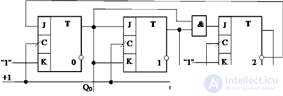
Fig. 4.34. Схема функциональная счетчика с М=5
В спроектированной схеме счетчика лишние состояния исключены в том смысле, что они не используются при нормальном функционировании счетчика. Но при сбоях или после подачи напряжения питания на схему в начале ее работы лишние состояния могут возникать. Поэтому полезно определить поведение схемы (автомата), в которой возникло лишнее состояние. Имея схему, можно полностью предсказать ее поведение во всех возможных ситуациях. Сделаем это для полученной схемы счетчика.
Взяв каждое лишнее состояние, найдем для него функции возбуждения триггеров, определяющие их переходы в следующее состояние. При необходимости найдем таким же способом следующий переход и т.д. В нашем случае лишними состояниями счетчика являются состояния 101, 110 и 111.
В состоянии 101 Q 2 =1, Q 1 =0 и Q 0 =1. Зная функции возбуждения триггеров, находим, что J 0 =0, K 0 =1, K 1 =J 1 =1, J 2 =0 и K 2 =1. Следовательно, триггеры 0 и 2 сбросятся, а триггер 1 переключится в противоположное состояние и из лишнего состояния 101 счетчик перейдет в состояние 010. Аналогичным способом можно получить результаты для состояний 110 и 111.
В итоге удобно построить диаграмму (рис. 4.35) состояний счетчика (граф переходов) в которой учтен не только рабочий цикл (его состояния показаны на рис. 4.35 кружками), но и поведение автомата, попавшего в неиспользуемые состояния (на рис. 4.35 показаны прямоугольниками). Из диаграммы видно, что рассматриваемый счетчик обладает свойством самозапуска (самовосстановление после сбоя) независимо от исходного состояния он приходит в рабочий цикл после начала работы. Этим свойством обладают не все схемы. В некоторых схемах автоматический вход в рабочий цикл не происходит.
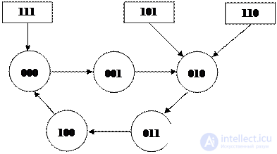
Fig. 4.35 Диаграмма состояний счетчика с модулем 5
Среди счетчиков с произвольным модулем особое место занимают двоично-десятичные счетчики, у которых модуль равен 10. Такие счетчики нетрудно построить формально проиллюстрированным выше методом. In fig. 4.36 представлена схема счетчика ИЕ2, которая появилась в самых первых сериях ИС и до сих пор повторяется во всех более новых сериях. Эта схема фактически состоит из двух секций: с модулем 2, представленной триггером Т 0 , и модулем 5, представленной группой Т 1 Т 2 Т 3 . Секции можно использовать по отдельности или соединять последовательно с помощью внешней коммутации выводов для получения двоично-десятичного счетчика. У данной микросхемы имеется сброс по конъюнкции сигналов R 0 R 1 и установка в состояние 1001 по конъюнкции сигналов S 0 S 1 .
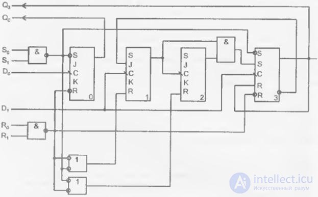
Fig. 4.36. Схема счетчика ИЕ2 серии КР1533
Соединение счетчиков в порядке mod2-mod5 дает двоично-десятичный счетчик с естественной последовательностью счета, который в режиме делителя частоты формирует импульсы со скважностью 5. Соединение в порядке mod5-mod2 дает тот же модуль счета, но состояния счетчика образуют последовательность чисел 0, 1, 2, 3, 4, 8, 9, 10, 11, 12, после которой цикл повторяется. В режиме делителя частоты формируются импульсы со скважностью 2. Таким образом, разбиение счетчика на две секции предоставляет возможность получить как обычный двоично-десятичный счетчик, так и два делителя частоты на 10 – с формированием узких импульсов (t и =Т/5) и симметричных импульсов (t и =Т/2), где Т – период повторения импульсов.
При управлении сбросом выявляется момент достижения содержимым счетчика значения М-1 . Это является сигналом сброса счетчика в следующем такте, после чего начинается новый цикл счета. Это вариант обеспечивает легкость перестройки счетчика на другие значения модуля, т.к. требуется изменить лишь код, с которым сравнивается содержимое счетчика для выявления момента сброса, т.е. не требуется изменений самой схемы счетчика.
Рассмотрим этот метод применительно к реализации синхронного счетчика с параллельным переносом на JK-триггерах. Функции возбуждения двоичного счетчика указанного типа, как известно, имеют вид J i =K i =Q 0 Q 1 …Q i -1 (в младшем триггере J 0 =K 0 =1). Введем в эти функции сигнал сброса R, изменив их следующим образом: J i =(Q 0 Q 1 …Q i -1 ) , K i = J i +R. Схема формирования функций возбуждения триггеров счетчика представлена на рис. 4.37.
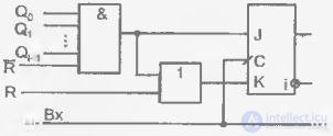
Fig. 4.37. Схема формирования функций возбуждения и ее подключение к
триггерам счетчика
Пока сигнал сброса отсутствует (R=0), функции J i и K i не отличаются от соответствующих функций двоичного счетчика. Когда сигнал R=1, все функции J i становятся нулевыми, а K i – единичными, что заставляет все триггеры сброситься по приходе следующего такта. Если сигнал R появится как следствие достижения в счетчике числа М-1, то будет реализована последовательность счета 0, 1, 2, …, М-1, 0, …, т.е. счетчик с модулем М.
Конъюнктор, входящий в состав схемы, тоже вырабатывает сигнал сброса, но при достижении содержимым счетчика значения М-1. В случае построения четырехразрядного двоично-десятичного счетчика на входы конъюнктора Q 0 Q 1 Q 2 Q 3 необходимо, соответственно подключить выходы счетчика  , что приведет к сбросу всех разрядов счетчика по пришествию сигнала счета, последующего после достижения счетчиком числа 1001 2 =9 10 , т.е. счетчик действительно работает как двоично-десятичный.
Распределители тактов тоже относятся к разряду счетчиков, но в отличие от счетчиков, рассмотренных ранее, особенностью этих счетчиков является то, что код, записанный в его разряды, не является двоичным, т.е. это счетчики с недвоичным кодированием . Наибольшее практическое значение среди таких счетчиков имеют счетчики с кодом «1 из N» или распределители тактов и счетчики Джонсона.
Основной областью применения распределителей тактов являются системы синхронизации и управления. На их основе получают импульсные последовательности с заданными временными диаграммами. Для этого можно вначале разбить период временной диаграммы на части («кванты»), соответствующие минимальному интервалу временной диаграммы, применив задающий генератор с частотой m/T , где m – число квантов в периоде T диаграммы. Выходные импульсы задающего генератора затем распределяются во времени и пространстве так, что каждый квант появляется в свое время и в своем пространственном канале.
На рисунке 4.38.а представлена структура распределителя тактов (РТ), согласно которой РТ имеет 1 вход, на который подаются импульсы с задающего генератора (ЗГ), и N выходов, причем первый импульс генератора передается на первый выход (канал) РТ, второй – на второй и т.д.
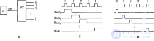
Fig. 4.38 Структура распределителя тактов (а) и временные диаграммы распределения уровней (б) и импульсов (в)
Распределители тактов бывают двух типов: распределители уровней (РУ) и распределители импульсов (РИ).
Временная диаграмма работы распределителя уровней представлена на рис. 4.38.б. Как видно из этой диаграммы паузы между активными состояниями каналов РУ отсутствуют.
Временные диаграммы, представленные на рис. 4.38.в, соответствуют работе распределителя импульсов. В данном распределителе тактов на выходе каждого канала появляется импульс, длительность которого соответствует длительности входных импульсов от ЗГ. Распределители импульсов не имеют самостоятельной схемотехники, они реализуются на основе распределителей уровней путем включения в их выходные цепи конъюнкторов, на вторые входы которых подаются импульсы задающего генератора.
Имея распределенные во времени и пространстве «кванты», можно по схемам ИЛИ собирать из них импульсные последовательности с необходимыми временными диаграммами. Часто нужны именно те последовательности, которые вырабатываются непосредственно распределителями тактов.
В общем случае распределители тактов могут быть получены в виде сочетания обычного двоичного счетчика и дешифратора . Такое решение наиболее очевидно. При большом числе выходных каналов эта структура может выигрывать у других, но при малом числе каналов преимущество по аппаратурной сложности и быстродействию, как правило, оказывается на стороне вариантов с кольцевыми регистрами или счетчиками Джонсона.
Одним из вариантов схемотехнического решения распределителя тактов, а точнее – распределителя уровней, является сдвигающий регистр, замкнутый в кольцо (кольцевой регистр сдвига), если записанное в этот регистр слово содержит всего одну единицу . При сдвигах единица перемещается с одного выхода на другой, циркулируя в кольце. Число выходов РТ равно разрядности регистра. In fig. 4.39 представлена структурная схема РТ на 3 выхода, в виде кольцевого регистра сдвига, созданного на синхронных D-триггерах.

Fig. 4.39. Структурная схема РТ на базе кольцевого регистра сдвига
Недостаток данной схемы состоит в потере правильного ее функционирования при сбое. Those. если в силу каких-либо причин слово (только одна единица) в регистре исказится, то возникшая ошибка будет постоянной, а это значит, что данная схема не обладает свойством самозапуска.
In fig. 4.40 представлена схема РТ на кольцевом регистре сдвига с самовосстановлением за несколько тактов. Работа этой схемы основана на том, что на вход регистра подаются нули, пока в нем имеется хотя бы одна единица. Таким образом, лишние возникшие единицы на его входе будут устранены и, когда регистр очистится, сформируется сигнал записи единицы на его входе. Следовательно, потеря единственной единицы также будет исключена. Выход ЛЭ, выполняющего самовосстановление схемы, дает еще один дополнительный канал. На схеме, приведенной на рис. 4.40, показаны также цепи пуска/останова РТ и два варианта выхода – для распределителя уровней (непосредственно с триггеров и ЛЭ ИЛИ-НЕ) и распределителя импульсов (после стробирования сигналов распределителя уровней импульсами сдвига на цепочке конъюнкторов).
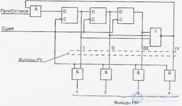
Fig. 4.40. Схема распределителя тактов с автоматическим вхождением в рабочий цикл
Можно поставить задачу более быстрого исправления сбоев, в том числе в ближайшем такте. Для этого необходимо задать и реализовать соответствующую диаграмму состояний распределителя. Сделаем это для трехканального распределителя. Диаграмма состояний с указанием рабочего цикла кружками и ложных состояний прямоугольниками приведена на рис. 4.41. Ей соответствует таблица истинности – табл. 4.7.
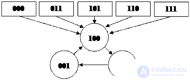
Fig. 4.41. Диаграмма состояний РТ с автоматическим вхождением в рабочий цикл за один такт
Таблица 4.7
| Q 1 | Q 2 | Q 3 | Q 1H | Q 2H | Q 3H | Q 1 | Q 2 | Q 3 | Q 1H | Q 2H | Q 3H |
Выбрав для построения схемы D-триггеры, учтем, что функция возбуждения этого триггера D=Q H . Исходя из таблицы истинности, для функций D i =Q iH имеем следующие соотношения:
 ,
,  and
and  .
.
Схема распределителя тактов с автоматическим вхождением в рабочий цикл за один такт представлена на рис. 4.42.
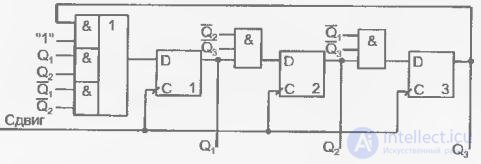
Fig. 4.42. Функциональная схема распределителя тактов с автоматическим вхождением в рабочий цикл за один такт
Распределители на кольцевых регистрах сдвига находят применение при малом числе выходных каналов, когда необходимость иметь по триггеру на каждый канал не ведет к чрезмерно большим аппаратурным затратам. Достоинством таких распределителей является отсутствие дешифраторов в их структуре и, как следствие, высокое быстродействие (задержка перехода в новое состояние равна времени переключения триггера).
Для увеличения количества выходных каналов РТ при том же количестве триггеров кольцевого регистра сдвига применяется кольцевой регистр сдвига с перекрестной обратной связью , который получил название счетчик Джонсона или Мёбиуса или Либау-Крейга . Такой счетчик имеет обратную связь на первый триггер от инверсии последнего триггера кольцевого регистра (рис. 4.43.а). Он имеет 2n состояний, т.е. при той же разрядности вдвое больше, чем обычный кольцевой регистр, а это значит, что с его помощью можно реализовать РТ с количеством выходных каналов в 2 раза больше по сравнению с РТ, реализованным на основе обычного кольцевого регистра сдвига. В то же время выход счетчика Джонсона представлен не в коде «1 из N», что требует преобразования кодов для получения выходов распределителя тактов. Такие преобразователи очень просты, что обуславливает применение счетчиков Джонсона в составе распределителей тактов.
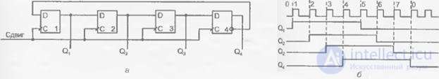
Fig. 4.43 Функциональная схема счетчика Джонсона (а) и временные диаграммы его работы (б)
Показанный на рисунке четырехразрядный счетчик Джонсона при начальном нулевом состоянии работает следующим образом. Первый импульс сдвига установит первый триггер в единичное состояние (  ), в остальных разрядах будут нули как результат сдвига нулей от соседних слева разрядов. Второй импульс сдвига сохраняет единичное состояние первого триггера, т.к. по прежнему . Второй разряд окажется в единичном состоянии, поскольку примет единицу от первого триггера. Остальные разряды будут нулевыми. Последующие сдвиги приведут к заполнению единицами всех разрядов счетчика, т.е. «волна единиц», распространяясь слева направо приведет счетчик в состояние 1111. Следующий импульс сдвига установит первый разряд в ноль, т.к. теперь
  . Этим начинается процесс распространения «волны нулей». После восьми импульсов повторится состояние 0000, с которого начато рассмотрение работы счетчика. Временные диаграммы описанных процессов показаны на рис. 4.43.б.
Особенность рассмотренной схемы – четное число состояний при любом количестве разрядов n счетчика, т.к. 2n – всегда число четное. Обычный кольцевой счетчик такого ограничения не имеет.
Преобразование выходного кода счетчика Джонсона в код «1 из N» требует добавления всего одного двухвходового элемента И либо И-НЕ для каждого выхода распределителя тактов. Принцип дешифрации состоит в выявлении положения характерной координаты временной диаграммы – границы между зонами единиц и нулей (табл. 4.8).
Таблица 4.8
| Номер состояния | Q 1 | Q 2 | Q 3 | Q 4 | Номер состояния | Q 1 | Q 2 | Q 3 | Q 4 |
В двух случаях (для слов, состоящих только из нулей или только из единиц) состояние выявляется анализом крайних разрядов. В остальных случаях анализируются разряды на границе зоны единиц и нулей.
Как видно из таблицы, преобразование выходного кода счетчика Джонсона в код «1 из N» осуществляется согласно следующим выражениям:
 ,
,  ,
,  ,
,  ,
,
 ,
,  ,
,  and
and  ,
,
где F i (i=0…7) – выходы распределителя тактов.
По полученным выражениям строится дешифратор. Рассмотрим дешифратор на ЛЭ И-НЕ (с инверсными выходами). В таком дешифраторе можно дополнительно принять меры по предотвращению перекрытий импульсов в соседних каналах, возможных из-за различных задержек элементов. Используя элементы с тремя входами и «косыми связями» (рис. 4.44.а) можно запретить начало импульса в последующем канале до его завершения в предыдущем.

Fig. 4.44. Функциональная схема дешифратора кода Джонсона в код «1 из N» (а), структурная схема распределителя тактов на основе счетчика Джонсона и временные диаграммы его работы (б)
Распределитель тактов в целом (рис. 4.44.б) имеет выходные сигналы в коде «1 из N».
Для схем со счетчиком Джонсона могут возникнуть вопросы преодоления ограничения обязательной четности числа состояний счетчика и обеспечения автоматического вхождения его в рабочий цикл (свойства самозапуска).
Первую задачу можно решить в рамках подхода, применявшегося при построении счетчиков с произвольным модулем, т.е. исключением одного «лишнего» состояния. Получить схему с исключенным состоянием можно уже не раз показанным способом, переходя от таблицы функционирования (истинности) к функции возбуждения триггеров и далее к схеме. Однако в данном случае нетрудно сократить этот путь, воспользовавшись простыми рассуждениями. Пусть исключению подлежит состояние 11..11. Чтобы его исключить необходимо перейти к следующему состоянию не из состояния «все единицы», а от предыдущего состояния 11…10, которое создает единицу в предпоследнем разряде счетчика, т.е. ноль на инверсном выходе этого разряда. Подавая нулевой сигнал на вход счетчика вместе с основным сигналом обратной связи через конъюнктор (показан на рис. 4.44.б штриховой линией) исключим состояние 11…11 и получим счетчик с нечетным числом состояний 2n-1.
The task of ensuring the occurrence of the distributor on the basis of the Johnson counter in the working cycle is related to the fact that the basic scheme, discussed above, does not have the property of self-starting. For example, a distributor with a three-digit Johnson counter has a total number of possible states of 2 3 = 8, and the number of states in a working cycle is 2 × 3 = 6. Two states are not used: 010 and 101. It is easy to notice that from state 010 the counter goes to state 101, and from state 101 to state 010. Thus, along with a closed working cycle, there is a cycle from two unused states without external influence will not be able to go into the working cycle.
In order to give the circuit the self-starting property, it is necessary to modify the feedback signal at the input of the counter. This can be done in different ways, since the trajectory of the transition from a closed cycle of unused states to the working state is ambiguous. One of the possibilities is to generate a feedback signal according to the expression
 .
.
Tactics distributors based on Johnson's counter are characterized by small hardware costs (1/2 trigger and one two-way valve per channel) and high enough speed (settling time = sum of trigger and valve switching delays). Johnson counters are implemented, in particular, in the series of ICs of the CMOS type (IE9 and IE19 chips of the K531 series, etc.), and one of the reasons for their use is the absence of impulse noise in the power circuit created by the chips. The clock allocator is generally implemented in the IC K561IE8.
1. Draw diagrams of bistable cells on LE-OR-NOT and NON and count their work.
2. Draw a classification scheme for triggers.
3. Draw timing diagrams of an asynchronous RS trigger with direct inputs.
4. Describe the differences between the R-flip-flop, S-flip-flop and E-flip-flop from the RS-flip-flop.
5. Draw a truth table JK-trigger.
6. Draw the functional diagrams of the synchronous RS-flip-flop in the basis of the OR-NOT and AND-NOT
7. Draw time diagrams of synchronous RS-trigger operation with synchronization along the leading and trailing edges.
8. Draw a functional diagram of the R-flip-flop based on the RS-flip-flop.
9. Draw a functional diagram of the JK-trigger based on the RS-flip-flop.
10. Draw a functional diagram of the D-trigger based on the JK-trigger.
11. Draw a functional diagram of the n-bit register on D - triggers.
12. Give the definition of the counter and describe the classification of counters.
13. Give the definition of the counting module of the meter, resolution, registration time and capacity.
14. Describe the various ways of implementing arbitrary counting modules in counters.
15. Draw time diagrams of operation of level and pulse distributors.
16. Draw a diagram of the level allocator based on the counter and decoder.
17. Draw a circuit of the pulse distributor on the basis of the ring shift register.
18. Draw a functional diagram of the Johnson counter and time diagrams of its work.

Comments
To leave a comment
Computer circuitry and computer architecture
Terms: Computer circuitry and computer architecture