Lecture
Having considered in the previous sections the basics of neuromathematics and the elemental base of neurocalculators, we will dwell in more detail on the analysis of the structural and functional construction of neural computations.
As noted in the first part of the review, a neurocomputer is a computer system with MSIMD architecture, i.e. with parallel streams of the same commands and multiple data flow. Today we can distinguish three main directions of development of computing systems with mass parallelism (VSMP):
| No | Name of direction | Description |
| one | VSMP based on cascade connection of universal SISD, SIMD, MISD microprocessors. | Element base - universal RISC or CISC processors: Intel, AMD, Sparc, Alpha, Power PC, MIPS, etc. |
| 2 | Based on processors with parallelization at the hardware level. | Element base - DSP processors: TMS, ADSP, Motorola, FPGA. |
| 3 | VSMP on specialized element base | Element base from specialized single-bit processors to neurochips. |
As noted in the first part of the review: neural network systems implemented on hardware platforms of the first direction (albeit multiprocessor) will be referred to as neuro-emulators - i.e. systems implementing typical neurooperations (weighted summation and nonlinear transformation) at the program level. Neural network systems implemented on hardware platforms of the second and third direction in the form of expansion cards of standard computing systems (1st direction) - we will call neuro accelerators and systems implemented on a hardware platform of the third direction in the form of functionally complete computing devices, should be referred to neurocomputers (all operations are performed in the neural network logical basis). Neuro accelerators can be divided into two classes: "virtual" (inserted into the expansion slot of a standard PC) and "external" (connecting to the host computer controlling via a specific interface or bus) [2-5]. Consider the principles of implementation and the basic structural and functional features of neurocalculators of the second and third types with specific examples.
The construction of FPGA-based neurocalculators, on the one hand, allows flexible implementation of various neural network paradigms, and, on the other, is associated with major wiring problems for all necessary interconnects. Currently available FPGAs have different functional capabilities (with the number of valves from 5 to 100 thousand). FPGA-based neurocomputers are generally positioned as flexible neural computing systems for research purposes and large-scale production. To build more efficient and effective neurocalculators, as a rule, the use of signal processors is required.
A large number of works presented at the last exhibition "Neurocomputers and their applications." We, as an example, consider the neurocalculator created at the Scientific Research Institute of Grain Research (RAS) [3].
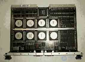
Fig.1. Appearance PPV.
A parallel reprogrammable computer (PPV) was developed in the VME standard and implemented on the basis of Altera 10K reprogrammable chips. The calculator is designed to work as a hardware accelerator and is a slave device on the VME bus. It should be included in the system as a slave device of the main control computer (host machine) with a universal processor. The clock frequency of the calculator is 33 MHz [3].
PPV is used to build image recognition systems based on the processing of television, thermal and other information, as well as systems based on the implementation of algorithms with threshold functions and the simplest arithmetic operations and allows you to achieve significant computational speed.
The calculator consists of the following functional blocks [3]:
The control circuit is used to control the BVE and data flows in the computer and is the simplest RISC processor. The structure and instruction set of the processor may vary depending on the type of task being solved.
BVE are used to perform simple arithmetic operations such as summation, subtraction, multiplication and calculation of threshold functions. Since BVE is implemented on reprogrammable microchips, their architecture may vary. The BVE architecture for different algorithms may differ, but is usually easily realized by combining library functions, compiling them using CAD (such as MaxPlus) and loading the configuration file into the selected BVE.
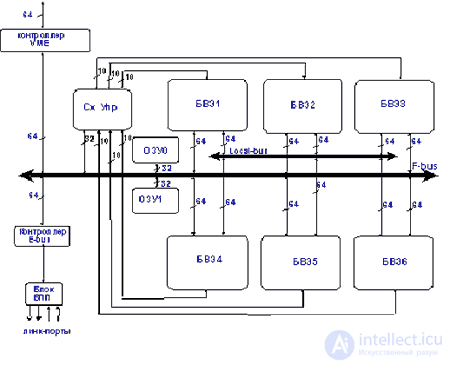
Fig.2. Block diagram of the PPV [3].
Two arrays of local static memory are assembled from 8 static memory chips with a capacity of 0.5 MB, have a size of 4 MB and are organized as an array of 512K 8-byte words. Memory arrays are associated with the control circuit of individual address buses and can function independently of each other. The memory is intended for storing common coefficients, as well as intermediate results of calculations or final results prepared for transmission via the system bus controller to the central processor or via the E-bus controller to the link ports.
The connection of several calculators among themselves or of the calculator with the image digitizing device, if the digitizing device has a corresponding interface, is carried out by means of a serial channel of CYPRESS receivers / transmitters. The data transfer control is performed by the external bus controller, which is a set of 4 standard FIFOs and control and data registers. The VME bus controller performs the interface function with the central processor and is a standard device.
From the point of view of the programmer, the calculator can be represented as a RISC processor (control circuit or control processor) and six vector processors (computational elements) working on SIMD commands (one com *** and for many data). A large number of data buses, the possibility of simultaneous operation of all BVEs and the execution of multiplication and addition arithmetic operations in a single clock cycle allows us to effectively parallelize the processing of information.
A feature of the control circuit of a reprogrammable computer for information processing systems is the presence of a working team that manages six basic computing elements. A com *** a allows simultaneously, for one clock cycle, setting various modes of operation for six basic computing elements and incrementing the addresses of both memory arrays by any number from 0 to 255 stored in increment registers, each register having its own register. Com *** and can be repeated any number of times in accordance with the value stored in a special register. This allows you to perform the main com *** with no loss on the organization of cycles and transitions. Working room *** a allows you to simultaneously run both local memory controllers, increment the address registers to the required value, set addresses from the corresponding address registers to address buses, and issue commands from the corresponding BVE registers to the BWE control buses. In addition, the working room *** and organizes the exchange of data between the controller external bus and local memory.
Table 1.
| Algorithm Name | Pentium-100, with | PentiumII-333, s | Ultra SPARC, c | PPV, with |
| Convolution with 4x4 core 3) | 0.65 | 0.11 | 0.76 | 0.02 |
| Median Filter | 1.97 | 0.49 | 0.75 | 0.001 |
| Contrast enhancement | 0.51 | 0.13 | 1.31 | 0.004 |
| Direct pointwise comparison with mask 32x32 4) | 43.78 | 7.14 | 58.89 | 0.142 |
| Search for local inhomogeneities 32x32 | 0.120 | 0.028 | 0.146 | 0.032 |
| Matrix multiplication by a matrix | 8.61 | 0.60 | 12.31 | 0.011 |
Ratings are given for:
Pentium-100 at a frequency of 100 MHz, the amount of RAM 16 MB;
Pentium-333 at a frequency of 350 MHz, 128 MB RAM;, br> UltraSPARC at a frequency of 200 MHz, 64 MB RAM;, br> Calculator at a frequency of 33 MHz.
The method of quick creation of FPGA neurocalculators is given in [6]. The main trends in the design of FPGA neurocalculators is an increase in the density of neurocrystals by reducing the area of interconnections and functional nodes of digital neurons. To solve this problem they find application:
Such neurocalculators are multiprocessor systems with the possibility of parallel processing, which makes it possible to realize neural computing systems on their basis, in the structure of which two main parts can be distinguished:
Let us dwell on the features of the hardware implementation of the neurocalculator (HB) with the possibility of parallel processing, realizing the elements of the neural network.
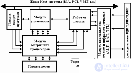
Fig.3. Generalized functional diagram of virtual NV.
The basis of the construction of the NV of this type is the use of signal processors, interconnected according to a specific architecture, which provides parallel execution of computational operations. As a rule, such HBs are built on the basis of a flexible modular architecture, which provides simplicity of the system configuration and increasing the computing power by increasing the number of processor modules or using more efficient signal processors (Fig. 3.). HB of this type are implemented mainly on the basis of carrier modules of the standards ISA, PCI, VME. Their main functional elements are the matrix signal processor (ICP) module, the working memory, the program memory, the signal input / output module (including the ADC, DAC and TTL lines), and the control module, which can be implemented on the basis of a specialized control signal processor (UE), based on the FPGA or have a distributed structure, in which general management functions are distributed among the SMEs.
To build HB of this type, the use of ADSP2106x, TMS320C4x, 8x, DSP96002 and other floating point signal processors is most promising.
Typical block diagram of the implementation of HB on the basis of the signal processor ADSP2106x is shown in Fig.4. [five]. It includes one control signal processor for performing general control functions, and up to eight processors performing parallel computations according to the algorithms in place (matrix signal processors).
The control and matrix processors form a cluster of processors with a common bus and shared memory resources. The exchange of information between the control processor, matrix processors, Host-computer and the external environment is carried out through the input / output ports. A debugging JTAG port is used for testing and debugging. Thus, in the case of four SMEs, information is exchanged between them and the UE through four connected ports of the ADSP2106x, two connected UE ports and the SME module are output to external connectors to provide communication with external devices. There are 12 external links, and 3 links of each of the SMEs are intended for intra-modular interprocessor exchange. Synchronization of the system can be carried out both from internal quartz oscillators and from external oscillators. Activation of software or external calculations.
A dedicated module is intended for input / output and AD / DAC signal conversions, which includes: a universal digital TTL port, ADC, DAC, a programmable voltage node for shifting the scale of the CTA and setting the trigger threshold of the starting comparators, the filtering node of the output signals, the testing subsystem , synchronization and control node, buffer memory FIFO. Initial loading is carried out on the Host interface or on links. The control interface of any SME allows you to control processor resets and interrupts, its identification number, etc.
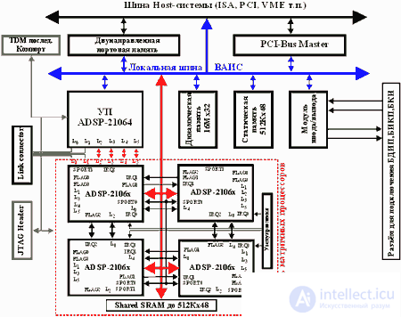
Fig.4. HB implementation based on ADSP2106x
This HB architecture provides real-time DSP operations, acceleration of vector calculations, the ability to implement neural network algorithms with high parallelism of vector and matrix operations.
The block diagram of HB based on the TMS320C4x signal processors is shown in Fig.5. Several DSPs included in the HB structure form a distributed computing structure from processor modules interconnected by high-speed ports. This embodiment of HB can be built using from two to eight signal processors.

Fig.5. HB structure based on TMS320C4x.
When using two parallel 32-bit DSP TMS320C40 information is exchanged when implementing neural network algorithms using six connected ports with a capacity of 30 Mb / s and DMA channels of each of the processors. Supporting parallel independent operation, the DMA subsystem and the processor provide parallel exchange of information at speeds up to 560 MB / s. Using high-speed ports, it is possible to implement on the basis of DSP data such architectures as: rings, hierarchical trees, a hypercube, etc. Each of the local buses TMS320C40 provides information exchange at speeds up to 120 MB / s.
The processor modules operate independently and, if necessary, are combined via connected ports. The exchange functions, control of processor modules, interrupts and DMA channels implement the FPGA, for example, from Xilinx. The use of dynamic reconfigurable structures (neural networks with structural adaptation) and the use of the latest FPGAs of the xC2xxx-xC4xxx families (Xinlinx) or similar ones requires minimizing the time for reconfiguring the FPGAs that are most often programmed in the Master Serial and Peripherial modes. The main disadvantage of using these reprogramming modes is the dependence of the FPGA reconfiguration process on the built-in clock generator. Minimal loss of time can be obtained when reconfiguring the FPGA in the Slave Serial mode, in which the internal clock is turned off and synchronization is performed via external clock signals. The FPGA reconfigurator is implemented as a specialized chip (for example, XC2018-84pin-50MHz, XC3020-68pin-50MHz).
The information storage subsystem includes modules of local static (up to 256Kx32) and dynamic memory (up to 8Мх32) for each of the processors and global static memory (up to 256Кх32). The host computer accesses global static memory with 16-bit words in the mode of line transfers with auto address incrementing by means of the address space of the I / O ports. To resolve possible conflict situations, access arbiters have been entered into the membership board. Additional information exchange can be carried out through the high-speed communication port. Host-computer has the ability to interrupt the operation of any of the processor modules. The interrupt subsystem supports interrupt handling to any of the DSPs when exchanging information with a Host-computer.
The implementation of NV, whose matrix processor unit is built on the basis of four TMS320C44 matrix with a capacity of 60 MFLOPS, is a distributed computing structure of processor modules with a capacity of up to 960 MFLOPS interconnected by high-speed ports. The structure of NV includes four ICPs (TMS320C44) TMS320C44), static memory (up to 512Кх32), dynamic memory (up to 16Мх32) and interface means for exchange with the external environment (Fig.4.). The processor used has two independent buses: global and local with an exchange rate of up to 240 MB / s and four parallel byte ports with a bandwidth of 30 MB / s. Communication ports provide interprocess communication with a minimum load on the microprocessor core, for which the corresponding DMA controllers for each of the ports are used. Each of the ports provides information transfer with a speed of up to 20 MB / s, which allows to achieve peak performance on all ports of about 120 MB / s.
Four processor modules operate independently on the board. The exchange of information between them is carried out by the byte port. Communication ports and DMA channels provide a variety of high-speed exchange capabilities. Host-computer has the ability to interrupt the operation of any of the processor modules. To use a specialized multi-window debugger for DSP tasks by Texas Instruments, a JTAG interface is introduced into the HB structure. Download programs and data, the exchange of data between HB and Host-computer is carried out through a high-speed communication port, which has a FIFO buffer in both directions. I / O nodes are connected via a global bus with a bandwidth of up to 100 MB / s. Channels of communication with the Host-computer fully meet the standard TIM-40, developed by a consortium led by Texas Instruments. The internal structure of the interface is determined by the configuration loaded into the FPGA.
Рассмотренные варианты НВ обеспечивают выполнение ЦОС и нейроалгоритмов в реальном масштабе времени, ускорение векторных и матричных вычислений, по сравнению с традиционными вычислительными средствами в несколько раз и позволяют реализовывать нейросеть с числом синапсов до нескольких миллионов.

Рис.6. Структура НВ на основе TMS320C44
Еще больше повысить производительность НВ данного типа можно при использовании одного из самых мощных на сегодня сигнальных процессоров - TMS320C80, TMS320C6ххх фирмы Texas Instruments.
Примером реализации нейровычислителя на DSP фирмы Моторолла является нейровычислитель NEURO TURBO фирмы Fujitsu. Он реализован на основе 4-х связанных кольцом 24-разрядных DSP с плавающей точкой МВ86220 (основные параметры: внутренняя точность 30 разрядов, машинный цикл 150 нс., память программ-25Кслов х2 (внутренняя), 64К слов х4 (внешняя), технология изготовления КМОП 1,2 мкм). Активационная функция нейронов ограничивается в диапазоне от 0 до 1, а возможные значения входов не превышают 16 разрядов, что обуславливает достаточную точность при 24-х разрядной архитектуре. Построение нейрокомпьютера на основе кольцевой структуры объединения DSP позволяет снизить аппаратные затраты на реализацию подсистемы централизованного арбитража межпроцессорного взаимодействия.
Нейрокомпьютер NEURO TURBO (рис.7) состоит из четырех DSP, связанных друг с другом посредством двухпортовой памяти. Каждый из DSP может обращаться к двум модулям такой памяти (емкостью 2К слов каждая) и к рабочей памяти (РП) (емкостью 64К слов х4 Банка) в своем адресном пространстве. Вследствие того что доступ к двухпортовой памяти осуществляется случайным образом одним из соседних DSP, то передача данных между ними происходит в асинхронном режиме. Рабочая память используется для хранения весовых коэффициентов, данных и вспомогательной информации. Для успешной работы НС необходимо получение сверток во всех элементарных нейронных узлах. Кольцевая структура объединения DSP обеспечивает конвейерную архитектуру свертки, причем передача данных по конвейеру осуществляется посредством ДПП. После того как DSP загружает данные из одной ДПП, он записывает результаты своей работы в смежную ДПП, следовательно, кольцевая архитектура параллельной обработки обеспечивает высокую скорость операции с использованием относительно простых аппаратных решений.
Для выполнения функций общего управления используется Host-ЭВМ на основе обычной вычислительной системы. Обмен данными между нейроплатой и Host-ЭВМ через центральный модуль ДПП. Загрузка программ в DSP осуществляется посредством памяти команд для каждого DSP. Следовательно, его архитектура полностью соответствует параллельной распределенной архитектуре типа MIMD. Пиковая производительность системы 24 MFLOPS.

Fig.7. Структура нейрокомпьютера NEURO TURBO (фирмы Fujitsu)
Для реализации модели НС иерархического типа фирмой Fujitsu выпущена нейроплата на основе DSP МВ86232, с собственной памятью до 4 Мб, что позволяет осуществлять моделирование НС, содержащей более 1000 нейронов. Структура НС включает в себя входной, промежуточный и выходной уровни (наибольшее число скрытых слоев - два (ограничение по памяти)). Для обучения нейрокомпьютера используются оригинальные фирменные алгоритмы: алгоритм виртуального импеданса, алгоритм скорректированного обучения и алгоритм расширенного обучения.
Каждая из рассмотренных типовых структур реализации НС может быть промоделирована на основе рассмотренных выше вариантов построения мультипроцессорных НВ. Так, для НВ на основе TMS320C4x при реализации какой-либо из рассмотренных архитектур (кольцо, иерархическое дерево, гиперкуб и т.п.) достаточно только изменить назначения коммуникационных портов, что обеспечивает гибкость и масштабируемость при исследовании и разработках нейросетевых систем различной архитектуры.
Если приведенное выше обобщенное описание реализации нейровычислительных систем Вас еще не утомило и Вы горите желанием попробовать что-то реализовать своими руками, то перед Вами встанет вопрос, а где взять "железо". Конечно, если вы работаете в крупном НИИ, то можно сделать и самим, а если вам необходимо уже готовое изделие? На рынке высокопараллельных вычислителей Москвы можно выделить следующие отечественные фирмы: во-первых, это АОЗТ "Инструентальные системы" (http://www.insys.ru) и НТЦ "Модуль" (http://www.mudule.ru), которые имеют целую линейку серийно производимых высокопараллельных вычислителей, во-вторых, это фирмы AUTEX Ltd (http://www.autex.ru), L-Card Ltd (http://www.lcard.ru) - производящие высокопараллельные вычислители , как правило под заказ на базе микропроцессоров Analog Devices, и фирма Scan (а точнее Scan Engeeniring Telecom (Воронеж)) - представляющая высокопараллельные вычислители на базе DSP фирмы Texas Instruments (http://www.scan.ru). Проанализируем продукцию некоторых из данных фирм в области высокопараллельных вычислителей на конкретных примерах.

Comments
To leave a comment
Computer circuitry and computer architecture
Terms: Computer circuitry and computer architecture