Lecture
Isolation amplifiers are designed for galvanic isolation of circuits directly connected to the source (sensor) of the signal and the circuits that process and transmit it to a memory or display device. This isolation is needed, for example, in applications such as
- medical devices to protect the patient from electric shock,
- when measuring in high voltage circuits,
- to reduce the error in the transmission of information with significant common-mode interferences on the signal transmission circuit.
To solve these problems, the measuring circuit is divided into two isolated parts. The transmitting part operates at the potential of the meter (sensor), and the receiving part - at zero potential. To implement such a device, it is necessary that the transmitting part has a separate, isolated from the receiving part, the so-called “floating” source of electrical energy.
The connection between these parts can be carried out by means of transformers, capacitors or optocouplers.
As an example, consider an isolating amplifier with a transformer coupling AD215, manufactured by Analog Devises (Fig.10.1).
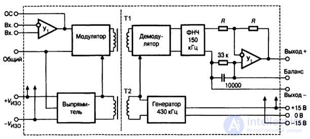
Fig.10.1. Isolation amplifier circuit with transformer coupling AD215
Here, to transmit the input signal through an isolation barrier, a balanced amplitude modulation of the carrier frequency of 430 kHz is used. The internal synchronizer controls the demodulator and transfers part of the energy through the transformer T2 to power the isolated part and control the modulator. A built-in isolated rectifier with a filter provides power to the isolated part of the circuit with a constant current of up to 10mA at a voltage of ± 15V.
The ripple voltage at the output of the demodulator is suppressed by a Bessel low-pass filter with a bandwidth of 150 kHz. As a result, the amplitude of the ripple of the output voltage of the amplifier does not exceed 5 mV. The bandwidth of the circuit is 0 ... 120kHz. If the bandwidth is limited to 50 kHz with an additional output filter, the amplitude of output voltage ripples will decrease to 1.2 mV. The nonlinearity of the transmission coefficient of the scheme with K = 1 does not exceed 0.015%.
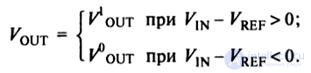
A comparator is a comparison device. An analog comparator is designed to compare the values of two analog signals. If we denote the input signal being analyzed as V IN , and the reference signal (or comparison level) V REF , then the output signal of the comparator, which is a logical signal, V OUT will be determined by the rule:
The output signal of the comparator in most cases is fed to the inputs of logic devices and therefore is consistent in level and power with their inputs.
An operational amplifier can be used as the simplest comparator (Figure 10.2). The amplifier is connected according to the inverting adder circuit, however, instead of a resistor in the feedback circuit, the Zener diode VD 1 and diode VD 2 are connected in parallel.
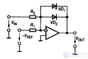
Fig.10.2. Comparator scheme at the OS
Let R 1 = R 2 . If (V IN - V REF )> 0, then the diode VD 2 is open and the output voltage of the circuit is equal to the voltage drop on the open diode and does not exceed 0.5 ... 0.7 V. At (V IN - V REF ) <0 at the zener diode a voltage equal to its stabilization voltage V ST will be established . This voltage should correspond to a single logic level of digital integrated circuits connected to the output of the comparator. Thus, the output of the op-amp takes two states, and in both the amplifier operates in linear mode.
The main purpose of reference voltage sources (ION) is to create a reference voltage that could be used by electronic information conversion devices as a reference. These devices include comparators, stabilizers, analog-digital and digital-analog converters, etc.
The simplest method of obtaining the reference voltage is that the unstabilized input voltage is applied through a current-limiting resistor to the zener diode, which plays the role of the so-called parametric stabilizer, whose main parameter is the breakdown voltage of the pn junction (Figure 10.3).
Volt-ampere characteristic of the Zener diode is shown in Fig.10.4.
Fig.10.3. ION circuit on zener diodes: a) parametric ION,
b) compensating type ion
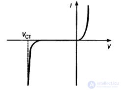
Fig.10.4. Voltage-current characteristic of the Zener diode
At a certain reverse voltage, called the stabilization voltage V ST , a breakdown of the pn junction occurs, and due to its design and technological features, this breakdown does not result in the failure of the device. The section of the current-voltage characteristic corresponding to the breakdown mode is located almost vertically, so that when the current through the Zener diode changes, the voltage on it changes little.
Stabilization quality is estimated by stabilization factor.
K ST = ΔV IN / ΔV REF
The stabilization factor for a parametric ION (fig.10.3a) can be 10 ... 100. In a compensating type ION, it can reach values of the order of 10,000.
Analog switches are used to switch analog signals. If the switch is in the “on” state, its output voltage should, as far as possible, be exactly equal to the input one, if the switch is in the “off” state, the output voltage should be as close to zero as possible.
There are various switch circuit solutions that meet the specified conditions. Their principle of operation is shown in Figure 10.5 for the example of mechanical (contact) switches.
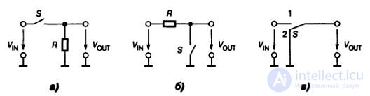
Fig.10.5. Mechanical switch diagrams: a) sequential,
b) parallel, c) series-parallel
The analog switches shown in Figure 10.5 can be implemented on electronic components with controlled resistance, having a small minimum and high maximum values. For these purposes, diode bridges, bipolar and field-effect transistors can be used. Due to imperfection, they introduce a series of static and dynamic errors into the switched signals. The main sources of error include:
- the pass resistance of the electronic key is not zero in the on state,
- the presence of non-zero residual voltage on a closed key with a zero switched signal,
- non-linear dependence of the resistance of the key on the voltage (current) on both the signal and control inputs,
- the mutual influence of the control and switched signals,
- the presence of a number of parasitic capacitances, some of which lead to the weakening of the high-frequency components of the switched signal when the key is closed, as well as between control and signal circuits,
- limited dynamic range of switched currents and voltages.
Keys on bipolar transistors and in particular on diode bridges consume significant power across the control circuits and have a relatively large residual voltage of a few mV, which introduces a noticeable error when switching weak signals (less than 100 mV). Such keys have high speed (the switching time of diode keys made on Schottky diodes reaches 1 nS) and is used to build ultra-high speed switches. In less high-speed switches, keys on field-effect transistors are much more widely used.
Schemes of switches with keys on MOS transistors are shown in Fig.10.6.
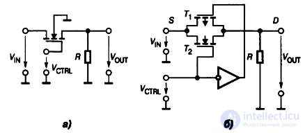
Fig.10.6. Serial switches with keys on MOS transistors: a) on n-channel MOS transistor, b) on CMOS transistors
The key in Figure 10.6a is intended for switching positive voltages that are at least 5 V less than V CTRL . When the gate-source voltage V GS ≤0, the channel resistance reaches tens of GΩ and the signal does not pass through the key. The supply to the gate relative to the source of a significant positive voltage translates the channel into a conducting state with a resistance of 1 to 300 ohms.
Keys on complementary MOS transistors (CMOS keys) have the best characteristics, Figure 10.6b. Here, the positive supply voltage + V S is supplied to the substrate of the VT 1 transistor, and the negative supply voltage –V S is supplied to the substrate of the VT 2 transistor.
With a high level of the control signal, the voltage at the gate of the n-channel transistor VT 2 is almost equal to + V S. In this case, the VT 2 transistor conducts signals with levels from –V S to only a few volts below + V S. At the same time, the voltage at the gate of the p-channel VT 1 is practically equal to –V S and it passes signals with levels from + V S to a value several volts above –V S. Thus, all signals in the range from –V S to + V S pass through parallel-connected VT 1 and VT 2 .
When the control signal is low, both transistors are locked.
This scheme works equally in two directions - its signal contacts S (source - source) and D (drain - drain) can serve as both input and output.
As an example of the use of analog keys, you can bring an analog multiplexer (Fig.10.7). It allows you to select one of several inputs corresponding to the address submitted to it. Such multiplexers are available either separately or can be built into an analog-to-digital converter or similar devices.
Each of the keys in Figure 10.7 from S 0 to S 3 is an analog CMOS switch. The decoder decodes the address represented in binary code and includes only the addressed key, blocking the rest. The permission input E is necessary to increase the number of switched signal sources, if a low level signal is sent to this input, then regardless of the state of the address inputs, all multiplexer keys are open. Since analog CMOS keys are bidirectional devices, analog multiplexes are simultaneously a demultiplexer, that is, the signal can be fed to the multiplexer output and removed from the selected input.
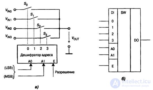
Fig.10.7. 4x1 analog multiplexer circuit: a) functional diagram, b) symbol
For complex commutation of analog audio and dideosignals, so-called crosspoint switches are used. They are used in cases when it is required to connect in a given configuration several signal sources with several receivers, including connections, in which several receivers are connected to one signal source. This is necessary for video servers, video transmission systems, video surveillance devices, video conferencing, audio applications, etc.
For example, Figure 10.8 shows the block-functional circuitry of 8x8 AD8108 / 09 matrix switches made by Analog Devises.

Fig.10.8. Block-functional circuit chip AD8108 / 09
Since it is possible to connect up to eight receivers to a signal source, output buffer amplifiers are used to reduce the load on the inputs. These amplifiers in the AD8108 have a single voltage gain, and in the AD8109 the gain of the buffer amplifiers is two.
The AD8108 / 09 chips use a matrix with 64 input stages, organized as eight 8x1 multiplexers. The outputs of this matrix switch are capable of operating at a standard 150 ohm video load with a low level of signal distortion (differential amplitude and phase errors do not exceed 0.02% and 0.02 °, respectively). The inputs have high resistance (10 MΩ) and low capacitance (2.5 pF). The outputs have low resistance (0.2 ohm at dc), but can be converted to a high impedance state (up to 10 MΩ).
The AD8108 / 09 switches are controlled in two ways: serial and parallel data entry. In the first case, a 32-bit control word is entered through the serial data input DATA IN, which fully defines the switch configuration. To change the state of a single key, you need to completely reprogram the matrix with a 32-bit word. With the parallel method, it is possible to switch one key by submitting a 7-bit word in the parallel code to the data inputs (4 lines) and addresses (3 lines) of the chip.
Analog Devises also produces 16x8 (AD8110 / 11) and 16x16 matrix switches (AD8113 / 14/15/15).
Optorele are similar to analog switches, but differ from them primarily by the lack of electrical connection between the control circuit and switched circuits. Electrical insulation voltage can reach several kilovolts. Optorele differ primarily in the types of key elements, which are used as thyristors, bipolar transistors and MOS transistors. The first two types of keys have poor accuracy characteristics, so the corresponding types of optolells are used exclusively for switching low-power circuits. Optorele with MOS transistors have good accuracy characteristics, so they can be used as commutators of analog channels. Fig.7.26 shows the scheme optorele on MOS transistors.
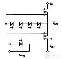
Fig.10.9. Circuit optorele on MOS transistors
The power switch consists of two MOSFETs with an n-type channel, connected in series with each other. Although this doubles the resistance of the open key, it allows you to get a high maximum allowable voltage in the closed state. The state control of both transistors is carried out by several photodiodes connected in series. Photodiodes work in this case as photo cells in idle mode. When illuminated, each of them produces a voltage of about one volt, so when I CTRL passes a current through the LED, the transistors open. Even in idle mode, the dynamic resistance of photodiodes is relatively high, so the processes of unlocking and locking the key associated with the charge of the input capacitance of the MOS transistors are rather slow.
A typical representative of this class of devices is the 2-channel TLV422 optorele of the International Rectifier company. This relay can provide switching of bipolar signals with voltages up to 400 V, which no CMOS switch allows. The maximum allowable insulation voltage is 4 kV. Resistance of the open channel is not more than 20 Ohm at the input control current of 5 mA. A typical key unlocking time with a switched current of 20 mA is 800 µs, and switching off time is 400 µs. The leakage current of the private key reaches 1 μA (for analog switches it is less than 1 nA).
The standard analog-to-digital conversion scheme provides for time sampling and subsequent level sampling. Time sampling is performed using sampling-storage devices (VHR), which are repeated at the output of the sampling (tracking) analog input signal, and when switching to storage mode, they store the last value of the input voltage until the next sampling signal arrives, that is, in essence They are analog storage devices. The stored signal (the current sample in time) is fed to an analog-to-digital converter (ADC) for conversion to digital form. For the ADC to work properly, it is necessary for the signal to be converted during the conversion time to remain constant. The scheme of the simplest SWH is shown in Figure 10.10a.
When the key S is closed, the output voltage of the circuit repeats the input, that is, V OUT = V IN (Fig.10.10b). When the key is opened, V OUT saves the value corresponding to the moment of opening. The output repeater on the op-amp prevents the discharge of the storage capacitor C H to the load of the circuit. The input impedance of the repeater should be as high as possible, therefore, usually used OU with field-effect transistors at the input. According to this scheme, for example, multichannel UVH SMP04 / 08 from Analog Devises was built.
UVH are available as separate microcircuits, or together with an ADC in one microcircuit.
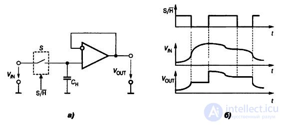
Fig.10.10. Sampling-storage device: a) schematic diagram,
b) timing charts
A digital-to-analog converter (DAC) is designed to convert a number, represented, as a rule, in the form of a binary code, into a voltage or current proportional to this number. Figure 10.11 shows the general classification of the DAC by the methods of converting the input code and the output signal generation schemes.
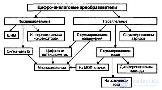
Fig.10.11. Generalized Classification DAC
Further classification of the DAC can be carried out according to a number of specific features, for example:
- by type of output signal: converters with current output or voltage output,
- by the type of digital interface: with serial input or with parallel input,
- by the number of DACs per crystal: single-channel and multichannel,
– по быстродействию: низкого, среднего и высокого быстродействия,
– по разрядности.
Наиболее простую конструкцию имеют параллельные ЦАП с суммированием весовых токов резистивными цепями (рис.10.12).
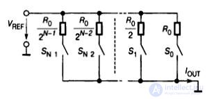
Рис.10.12. Простейшая схема ЦАП с суммированием весовых токов
В этой схеме сопротивления резисторов выбирают так, чтобы при замкнутых ключах через них протекал ток, соответствующий весу разряда. Ключ должен быть замкнут тогда, когда соответствующий ему бит входного кода равен единице. Выходной ток определяется соотношением
где k – разрядность входного кода, d k принимает значение 0 или 1 в зависимости от состояния k-го разряда входного тока, D – входной код
( точнее, суммарный вес входного кода). При высокой разрядности ЦАП токозадающие резисторы должны быть согласованы с высокой точностью. Наиболее жёсткие требования по точности предъявляются к резисторам старших разрядов, поскольку разброс весовых токов не должен превышать доли тока младшего разряда.
Рассмотренная схема ЦАП с суммированием весовых токов при всей её простоте обладает рядом недостатков:
– при различных входных кодах ток, потребляемый от источника опорного напряжения (ИОН), будет различным, а это может повлиять на величину выходного напряжения ИОН,
– значения сопротивлений весовых резисторов могут различаться в тысячи раз, что делает весьма затруднительной реализацию этих резисторов в полупроводниковых микросхемах; кроме того, сопротивление резисторов старших разрядов может быть соизмеримым с сопротивлением замкнутых ключей, а это ведёт к дополнительным погрешностям преобразования,
– в этой схеме к разомкнутым ключам прикладывается значительное напряжение, что усложняет их построение.
В настоящее время разными фирмами выпускается большое количество ЦАП, основанных на разных принципах, которые тем или иным образом обходят эти недостатки и обеспечивают высокие характеристики по точности и быстродействию.
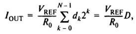
В схеме устройства ЦАП появляется тогда, когда необходимо обработанный цифровой сигнал преобразовать в аналоговую форму и подать на исполнительное устройство, которым может быть динамик, электродвигатель и т.п. Другим использованием ЦАП является прямой синтез сигналов необходимой формы, который предварительно формируется в цифровом виде, а затем с помощью ЦАП преобразовывается в аналоговый вид. Для примера на рис.10.13 приведена упрощённая схема генератора прямого цифрового синтеза (ПЦС) синусоидального сигнала с широким диапазоном задаваемых частот.
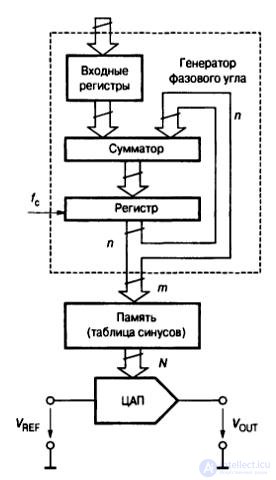
Рис.10.13. Упрощённая схема генератора ПЦС синусоидального сигнала
Схема прямого цифрового синтеза содержит три основных блока: генератор фазового угла, память и ЦАП. Генератор фазового угла в типичном случае представляет собой накапливающий сумматор с регистром. Работает он просто как регистр фазы, содержимое которого получает приращение на некоторый фазовый угол через заданные интервалы времени. Необходимое приращение фазы Δφ в виде цифрового кода загружается последовательно или побайтно во входные регистры. Память играет роль таблицы функций.
Системы прямого цифрового синтеза чрезвычайно гибки. Частота выходного сигнала может быть изменена практически мгновенно без разрыва фазы простым изменением содержимого входных регистров.
Преобразование сигналов из аналоговой формы в цифровую предполагает две операции. Первая – дискретизация по времени. Она осуществляется с помощью устройств выборки-хранения, рассмотренных ранее. Вторая – дискретизация по уровню. Для этого предназначены аналого-цифровые преобразователи (АЦП).
В простейшем случае АЦП представляют собой набор компараторов и логическое устройство, выдающее на выходе код, зависящий от того, какие компараторы сработали. На рис.10.14 показана схема такого 3-х разрядного АЦП. Подобные АЦП называются параллельными.
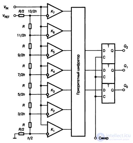
Рис.10.14. Схема параллельного АЦП
Весь диапазон входного сигнала разбит на восемь уровней, которые можно закодировать тремя двоичными разрядами. В соответствии с этими уровнями сформировано семь пороговых напряжений, которые подаются на семь компараторов. Все компараторы сравнивают входной сигнал со своим порогом. Входному сигналу сопоставляется цифровой код, соответствующий максимальному номеру компаратора, из тех, что сработали. Если ни один компаратор не сработал, то на выход подаётся код 000. Логическая схема, формирующая выходной код состоит из приоритетного шифратора и трёх триггеров, в которые записывается выходной сигнал импульсами синхронизации.
Благодаря одновременной работе компараторов параллельный АЦП является самым быстрым. Например, восьмиразрядный преобразователь MAX108 позволяет производить 1,5 млрд преобразований в секунду. Недостатком этой схемы является большой объём и сложность реализации. N-разрядный параллельный АЦП должен содержать 2 N -1 компараторов и 2 N согласованных прецизионных резисторов. Так, например, АЦП AD9060 содержит 512 компараторов.
Поэтому для приложений, где не требуется максимальная скорость преобразований, производится обмен быстродействия на экономию оборудования за счёт тактирования работы АЦП и использования одних и тех же компараторов для определения разных разрядов. В самом медленном варианте остаётся один компаратор, с помощью которого определяются все разряды (рис.10.15).
Рис.10.15. АЦП последовательного счёта: а) структурная схема,
б) временная диаграмма работы
Схема содержит счётчик, на который поступают счётные импульсы от генератора тактовых импульсов (ГТИ). Код, сформированный в счётчике поступает в ЦАП, выходной сигнал которого используется в качестве порогового для компаратора. Код в счётчике начинается с нулевого и потактно возрастает на единицу. Как только сработает компаратор, подача импульсов на счётчик прекращается и достигнутый код подаётся на выход. На следующем цикле обработки на вход компаратора поступает очередное значение V IN , счётчик сбрасывается в ноль и подача импульсов на счётчик возобновляется.
В настоящее время известно большое число методов преобразования напряжение-код. Эти методы существенно отличаются друг от друга потенциальной точностью, скоростью преобразования и сложностью аппаратной реализации. На рис.10.15 представлена классификация АЦП по методам преобразования.
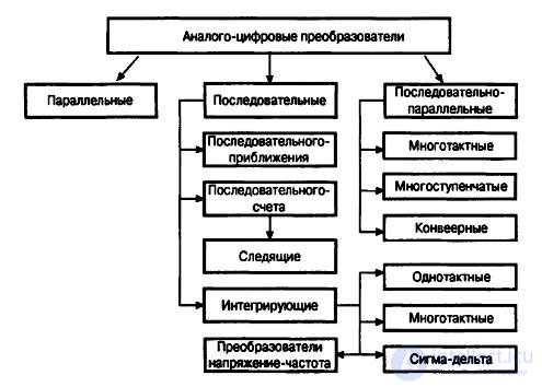
Рис.10.15. Классификация АЦП
Выбор АЦП для использования осуществляется адекватно приложению с учётом необходимых точности, быстродействия, потребления, габаритов и допустимой стоимости.
Постепенное усложнение АЦП, появление многоканальных АЦП, АЦП со встроенным устройством выборки-хранения, АЦП со сложной цифровой частью привело к тому, что сейчас имеются законченные однокристальные системы сбора данных, обеспечивающие преобразование в цифровой код сигналов, поступающих от многих датчиков и передачу их на микро-ЭВМ. Структурная схема развитой системы сбора данных приведена на рис.10.16.
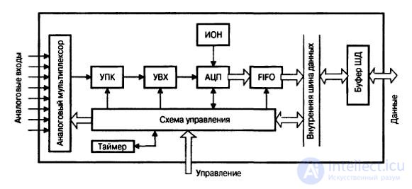
Рис.10.16. Структурная схема системы сбора данных
( УПК – усилитель с программируемым коэффициентом усиления, УВХ – устройство выборки-хранения, ИОН – источник опорного напряжения, ШД – шина данных)
В схему встроены устройство выборки-хранения и источник опорного напряжения. Для подключения к нескольким источникам входных аналоговых сигналов используется аналоговый мультиплексор. Чтобы сократить частоту прерываний главного процессора некоторые схемы сбора данных снабжаются оперативным запоминающим устройством типа FIFO (first input – first output, первый вошёл, первый вышел). Измерительный усилитель с программируемым коэффициентом усиления (УПК), входящий в систему, меняет свой коэффициент усиления по команде от схемы управления. Это позволяет выровнять диапазоны аналоговых сигналов с различных входов.
Примерами таких систем сбора данных могут служить, например, микросхемы AD7581, AD1B60 и LM12458.
1. Схема изолирующего усилителя с трансформаторной связью и описание его работы.
2. Схема компаратора на ОУ.
3. Diagram of the source of the reference voltage at the Zener diode and the compensation type.
4. Schemes of mechanical switches and switches with keys on MOS transistors.
5. Functional diagram of the analog multiplexer 4x1 and its symbol.
6. Circuit optorele on MOS transistors.
7. Functional diagram of the sampling-storage device and time diagrams of its operation.
8. The simplest DAC scheme with the summation of weight currents.
9. Simplified diagram of the generator of direct digital synthesis of a sinusoidal signal.
10. Scheme of the parallel ADC.
11. Block diagram of the ADC of the sequential count and the timing diagram of its work.
12. Classification ADC.
13. Block diagram of the data collection system.

Comments
To leave a comment
Computer circuitry and computer architecture
Terms: Computer circuitry and computer architecture