Lecture
The development of computer architecture, aimed at increasing their productivity, in recent decades has gone along the path of complicating processors by expanding the system of instructions, introducing complex commands that perform procedures that approach the primitives of high-level languages, increase the number of addressing methods used, etc.
However, the expansion and complexity of the command set causes a number of undesirable side effects. The expansion of the instruction set, the number of ways of addressing, the introduction of complex commands is accompanied by an increase in the length of the command and, first of all, an operation code, which leads to an increase in the number of command formats. This causes complication and slowing down the process of decoding the operation code and other procedures for processing instructions in the processor. The increasing complexity of command processing procedures makes it necessary to use firmware control devices with control memory (firmware CUs) instead of faster CPUs with rigid logic. The complication of the processor makes it more difficult and even impossible to implement it on a single LSI chip. And placing the processor in a single chip by reducing interconnect lengths makes it easier to achieve high performance.
The above explains why in the early 80s. An alternative direction has emerged in relation to the complexity of the processor architecture. When creating relatively cheap high-performance computers, it uses an architecture with a reduced set of commands (SNK-architecture), called in the foreign literature RISC-architecture. Below are only the basic principles underlying the classic RISC architecture.
RISC-architecture involves the implementation in the computer of a reduced set of simplest, but often used commands. This allows you to simplify the processor hardware and get the opportunity to increase its speed. When using the RISC architecture, the selection of instruction set and processor structure is directed to ensure that the instruction set is executed in one machine cycle of the processor. Execution of more complex but rarely encountered operations is provided by subroutines.
In a RISC-computer, a machine cycle is the time during which two operands are taken from the registers, the operation in the ALU is performed, and the results are stored in the register. Most of the commands in RISC are quick register-register commands and are executed without recourse to the OP. In order for this to be possible, the processor must contain a sufficiently large number of general registers.
Thus, RISC-architecture computers have a number of characteristic features:
- abbreviated instruction set (usually no more than 50-100);
- a small number (usually 2-3) of simple ways of addressing;
- a small number of simple command formats with fixed sizes and functional purpose of the fields.
All this simplifies the CPU's CU and makes it possible to dispense with the firmware level of control and control memory, i.e. CU can be executed on high-speed rigid logic.
The above features inherent in the RISC computer architecture, lead to such a significant simplification of the processor that it is possible to place in a single chip not only the processor, but also a large number of common registers. In modern BIS MP RISC architecture, the number of general and specialized registers reaches tens and hundreds, with a significant reduction in the total number of processor transistors. For example, to implement 32-bit RISC architecture processors, corresponding to the performance of class I80386 processors, less than 50,000 transistors are required, while for traditional architecture processors (CISC), more than 150,000 are required.
A large number of RON, especially in the presence of an optimizing compiler that ensures their effective use, makes it possible to reduce the appeal to the OP to the limit. This is achieved:
- due to the fact that the intermediate result of the calculation is stored on the registers;
- the transfer of operands from one program to another or a subprogram is carried out through registers;
- it is not required to transfer the contents of registers during interrupts to be saved in the OT
One of the characteristic features of the RISC architecture is the extensive use of the mechanism of overlapping register windows . It is designed to reduce the number of calls to the OP and interregister transmissions, which contributes to improving the performance of computers.
Procedures are dynamically allocated to small groups of fixed-length registers (register windows). The windows of sequentially executed procedures overlap, making it possible to transfer parameters from one procedure to another. When the procedure is called, the processor switches to work with another register window. In this case, there is no need to transfer the contents of the registers to memory.
The window consists of three subgroups of registers (Fig. 24.1).
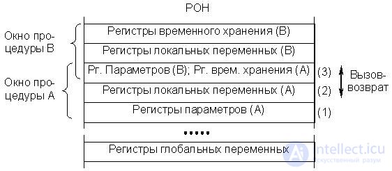
Fig.24.1. RISK - computer architecture. Overlapping register windows
We believe that the procedure call comes from the bottom up, i.e. Procedure A calls Procedure B, and has itself been called by some previous procedure. The first subgroup contains the parameters passed to this procedure (A) from its caller, and the results for the calling procedure when returning to it. The second subgroup contains local variables of procedure A. The third is a buffer for two-way exchange between procedure A and its procedure B. Procedure A transmits B parameters when called. When returning from procedure B to procedure A, the latter receives through this buffer the results of operation of procedure B. Thus, the same subgroup for procedure A is the temporary storage registers, and for the next (procedure B) the parameter registers. A separate window accessible to all program procedures is allocated for its global variables.
It should be noted that there are relatively few computers that fully meet the definition of RISC architecture. In most cases, these are computers close to the RISC architecture. For example, one of the first computers of this type was a high-performance PC from IBM PC-RT. He had 118 commands, only two ways of addressing and two formats of commands, 16 RON, the average number of cycles per command is three. The purely RISC-architecture is used to refer the processors of the Alpha series of the DEC company, the Power PC processor series of the joint development of Motorola, EPL, IBM, the Rxxxx series of processors (R4000, R5000, R10000) of the PA company. firms Hewlett Packard, a series of processors "SPARC" firm Sun Microsystems, etc.
Despite the widespread use of the terms "RISC" and "CISC" in the literature, architectures of modern powerful processors are difficult to unambiguously classify. This is due to the rapid complication of crystals of processors of both types of architectures (RISC and CISC), as well as the fact that in order to increase productivity, developers combine design solutions characteristic of both types of architectures in one device. So, in powerful CISC processors, it has become common to use the RISC core, which allows you to execute complex processor instructions as sets of elementary instructions implemented according to the principles of the RISC architecture.
It should also be noted that the principles of the RISC architecture are embedded in the ideology of building transputers , which form the basis of modern matrix processors used in supercomputers, as well as in “accelerator” boards for personal computers.
Despite the intensive use of RISC-architecture in serial samples of computers, the controversy continues around the advantages and disadvantages of this architecture. The latter, in particular, include the greater length of the program code after compilation (object code) as compared with the length of the code of machines of conventional architecture. So, when emulating VAX computer commands, on average, 5-6 commands of RISC-architecture machines are required for each of its commands. However, as studies have shown, the gain in the speed of command execution blocks the loss from the elongation of the object code (in general quality indicators of a computer).
As an example of RISK architecture, consider ARM processors, which account for more than 90% of all embedded 32-bit RISK processors. These processors have low power consumption and high performance, which determines their widespread use in devices such as PDAs (personal digital assistants), mobile phones, digital media and players, portable game consoles, calculators, and computer peripherals such as hard drives or routers .
ARM processors (Advanced RISK Machine — Advanced RISK Machine) are developed by UK-based ARM and its licensees. The ARM company itself is not engaged in the production of microcircuits, but sells ready-made solutions for the processor core to other companies that attach their peripherals to the core and are engaged in the production of microcircuits and devices based on them.
Currently, ARM manufactures the following processor families: ARM7, ARM9, ARM10, ARM11 and Cortex. Announced preparations for release in 2012 of the ARM A15 family, codenamed Eagle.
ARM A15 processors will have the following characteristics: clock speed up to 2.5 GHz, one, two, four or eight cores, support for 1 terabyte of RAM, ECC cache L1 and L2, common cache for multiprocessor systems, support for virtualization, double check of operations floating point, vector instructions, cache tracking.
In some models, future ARM chips promise to support multithreading technology, which will allow each core to process more than one instruction stream simultaneously.
Under the license of ARM, microprocessors such as Atmel, Cirrus Logic, Intel, Marvell, NXP, STMicroelectronics, Samsung, Qualcomm, Sony Ericsson, Texas Instruments, nVidia, Freescale, Analog Devises and others are manufactured by microprocessors. Examples of processors developed by major licensees: DEC StrongARM, Freescale i.MX, Marvell XScale, NVIDIA Tegra, ST-Ericsson Nomadik, Qualcomm Snapdragon and Texas Instruments OMAP.
The ARM architecture contains the following features of RISC:
One of the significant differences between the ARM architecture and other processor architectures is the so-called predication - the possibility of conditional execution of commands. By "conditional execution" is here meant that the command will be executed or ignored, depending on the current state of the processor state flags.
While for other architectures, only conditional branching commands, as a rule, have this property, the ARM architecture has incorporated the ability to conditionally execute almost any command. This was achieved by adding a special 4-bit field ( predicate ) to their instruction codes. One of its values is reserved so that the instruction can be executed unconditionally, and the rest encode one or another combination of conditions (flags). On the one hand, given the limited overall length of the instruction, this reduced the number of bits available to encode the offset in the memory reference commands, but on the other, it allowed us to get rid of branch instructions when generating code for small if-blocks.
The ARM processor also has some features that are rarely found in other RISC architectures, such as addressing relative to the program counter (in fact, the ARM command counter is one of 16 registers), as well as pre- and post-incremental addressing modes.
ARM7 and earlier versions have a three-stage conveyor. These are the stages of transfer, decoding, and execution. More productive architectures, such as ARM9, have more complex pipelines. Cortex-a8 has a 13-step conveyor.
The architecture provides a way to extend the instruction set using coprocessors, which can be addressed using register exchange commands with the MCR, MRC, MRRC, MCRR co-processors, and similar commands. The coprocessor space is logically divided into 16 coprocessors with numbers from 0 to 15, with the 15th reserved for some typical management functions, such as cache management and MMU operations (memory management unit).
In ARM-based machines, peripherals are usually connected to the processor by matching their physical registers in the ARM memory or in the memory of the coprocessor, or by connecting to buses, which in turn are connected to the processor. Access to coprocessors has a longer wait time, so some peripherals are designed to access in both directions. In other cases, chip developers only use the coprocessor integration mechanism. For example, the image processing engine should consist of a small core ARM7TDMI, combined with a coprocessor that supports primitive operations for processing elementary encodings HDTV (High-Definition Television-High Definition Television).
ARM provides 31 32-bit general-purpose registers. Depending on the mode and state of the processor, the user has access only to a strictly defined set of registers. In ARM state, 17 registers are constantly available to the developer:
In all modes except User mode and System mode, the Saved Program Status Register (SPSR) is also available. After an exception occurs, the CPSR register is stored in SPSR. This fixes the processor state (mode, state; flags of arithmetic, logical operations, interrupt enable) at the moment immediately before the interrupt
In most of the existing models of microprocessors PCI bus and the ability to work with external dynamic random access memory (DRAM) is implemented. Processors designed for consumer devices also usually integrate: USB bus controllers, IIC, AC'97-compatible audio device, a device for working with SD and MMC flash media, and a serial port controller.
All processors have general purpose input / output (GPIO) lines. In consumer devices, quick-start buttons, signal LEDs, a scroll wheel (JogDial), and a keyboard can be connected to them.
Thumb (Thumb / Stand)
To improve the compiled code density, the processors, starting with ARM7TDMI, are equipped with a thumbnail mode (in the original, the words arm - hand and thumb - are beaten around the thumb ). In this mode, the processor executes 16-bit instructions. Most of these 16-bit thumbs commands are translated into normal ARM commands. Space is saved by hiding some operands and limiting the possibilities compared to the full ARM instruction set mode.
In thumbs mode, smaller opcodes have less functionality. For example, only branches can be conditional, and many opcodes have access restrictions on only half of the main processor registers. Shorter opcodes generally give a higher code density, although some operations require additional commands. In situations where the memory port or bus width is limited to 32 bits, the shorter operation code of the thump mode becomes much more efficient compared to the usual 32-bit ARM code, since the smaller program code will have to be loaded into the processor with limited memory bandwidth.
Thumb-2
Thumb-2 is a technology launched from the ARM1156 core, announced in 2003. It expands the limited 16-bit Thumb command set with additional 32-bit commands to give the command set an extra width. The goal of Thumb-2 is to achieve code density like Thumb, and performance like a 32-bit ARM instruction set. It can be said that in ARMv7 this goal was achieved.
Thumb-2 extends both the ARM commands and the Thumb commands with even more commands, including control of the bit field, table branching, and conditional execution. The new language Unified Assembly Language (UAL) supports the creation of commands for both ARM and Thumb from the same source code.
Jazelle
Jazelle is a method that allows Java bytecodes to be executed directly in the ARM architecture as the 3rd execution state (and instruction set) along with the usual ARM commands and slider mode. Support for this property is indicated by the letter “J” in the processor name — for example, ARMv5TEJ. Необходимость такой поддержки появляется начиная с процессоров ARMv6, хотя новые ядра лишь содержат тривиальные реализации, которые не поддерживают аппаратного ускорения.
Усовершенствованный SIMD(NEON)
Расширение усовершенствованного SIMD, также называемое технологией NEON — это комбинированный 64- и 128-битный набор команд SIMD (single instruction multiple data), который обеспечивает стандартизованное ускорение для медиа приложений и приложений обработки сигнала. NEON может выполнять декодирование аудио формата mp3 на частоте процессора в 10Мгц, и может работать с речевым кодеком GSM AMR (adaptive multi-rate) на частоте более чем 13Мгц. Он обладает внушительным набором команд, отдельными файлами регистра, и независимой системой исполнения на аппаратном уровне. NEON поддерживает 8-,16-,32-,64-битную информацию целого типа, одинарной точности и с плавающей точкой, и работает в операциях SIMD по обработке аудио и видео (графика и игры). В NEON SIMD поддерживает до 16 операций единовременно.
VFP
Технология VFP (Vector Floating Point, вектора чисел с плавающей запятой) — это расширение сопроцессора в архитектуре ARM. Она производит низкозатратные вычисления над числами с плавающей запятой одинарной двойной точности, в полной мере соответствующие стандарту ANSI/IEEE Std 754—1985 Standard for Binary Floating-Point Arithmetic.VFP производит вычисления с плавающей точкой, подходящие для широкого спектра приложений — например, для КПК, смартфонов, сжатия звука, 3д-графики и цифрового звука, а также принтеров и телеприставок. Архитектура VFP также поддерживает исполнение коротких векторных команд. Но, поскольку процессор выполняет операции последовательно над каждым элементом вектора, то VFP нельзя назвать истинным SIMD набором инструкций. Этот режим может быть полезен в графике и приложениях обработки сигнала, так как он позволяет уменьшить размер кода и выработку команд.
Other floating point and / or SIMD coprocessors found in ARM processors include FPA, FPE, iwMMXt. They provide the same functionality as VFP, but are not compatible with it at the opcode level.
Security Extensions
Расширения безопасности, позиционируемые как TrustZone Technology, находятся в ARMv6KZ и других, более поздних, профилированных на приложениях архитектурах. Оно обеспечивает низкозатратную альтернативу добавлению специального ядра безопасности, обеспечивая 2 виртуальных процессора, поддерживаемых аппаратным контролем доступа. Это позволяет ядру приложения переключаться между двумя состояниями, называемыми «миры» (чтобы избежать путаницы с названиями возможных доменов), чтобы не допустить утечку информации из более важного мира в менее важный. Этот переключатель миров обычно ортогонален всем другим возможностям процессора. Таким образом, каждый мир может работать независимо от других миров, используя одно и то же ядро. Память и периферия соответственно изготавливаются с учетом особенностей мира ядра, и могут использовать это, чтобы получить контроль доступа к секретам и кодам ядра. Типичные приложения TrustZone Technology должны запускать полноценную операционную систему в менее важном мире, и компактный, специализированный на безопасности, код в более важном мире, позволяя Digital Rights Management'у намного точнее контролировать использование медиа на устройствах на базе ARM, и предотвращая несанкционированный доступ к устройству.
Отладка
Все современные процессоры ARM включают аппаратные средства отладки, так как без них отладчики ПО не смогли бы выполнить самые базовые операции типа остановки, отступа, установка контрольных точек после перезагрузки.
Архитектура ARMv7 определяет базовые средства отладки на архитектурном уровне. К ним относятся точки останова, точки просмотра и выполнение команд в режиме отладки. Такие средства были также доступны с модулем отладки EmbeddedICE. Поддерживаются оба режима — остановки и обзора. Реальный транспортный механизм, который используется для доступа к средствам отладки, не специфицирован архитектурно, но реализация, как правило, включает поддержку JTAG.
Архитектура ядра ARM7TDMI приведена на рис.24.2.
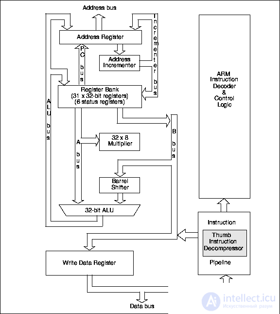
Рис.24.2. Упрощённая архитектура ядра ARM7TDMI
Ядро ARM7TDMI стало первым Thumb-ориентированным ядром. Это ядро семейства ARM7 располагающее:
– встроенной макроячейкой EmbeddedICE™, поддерживающей отладку встроенного ядра ,
– 32-разрядным аппаратным умножителем ,
– декомпрессором Thumb,
– 32-разрядной производительностью в 8- и 16-разрядных управляющих применениях .
Ядро ARM7TDMI пополнило стандартный ряд 32-разрядных ядер ARM, обеспечив возможность выхода на рынок встраиваемого управления, привнося 32-разрядную производительность в 8 и 16-разрядные применения управления. Первый Thumb-ориентированный прибор в кремнии был выпущен во второй половине 1995.
Ядро ARM7TDMI используется как лицензионная макроячейка ARM, предназначенная использования при создании стандартных приборов специального назначения .
И ARM7 и ARM7T ядра в одном тактовом цикле, используют 3-уровневый конвейер с фазами выборки, декодирования и выполнения
( рис.24.3). Поток команд через каждый уровень конвейера управляется высокими и низкими фазами тактового сигнала. В ядре ARM7TDMI неиспользуемая фаза тактового сигнала используется для декомпрессирования команд Thumb в каскаде декодирования. Следовательно, в одном тактовом цикле производится и декодирование и выполнение команды, не требуется никаких дополнительных непроизводительных затрат синхронизации.
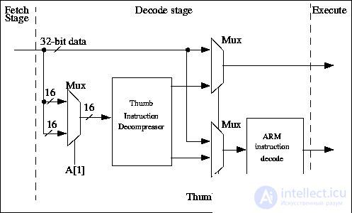
Рис.24.3. Thumb декодирование и декомпрессия
Команды ARM, поступающие из каскада выборки конвейера, проходят через декодер ARM и активируют сигналы управления старшими и младшими битами операционного кода. Старшие биты опкода описывают тип выполняемой команды, тогда как младшие биты определяют детали команды типа определения регистров или операнда.
В Thumb состоянии мультиплексоры направляют Thumb команды через логику декомпрессии Thumb, разворачивающую команду Thumb в ее эквивалент ARM команды . Затем команда ARM выполняется в нормальном режиме.
Блок-схема ядра ARM1020T семейства ARM10 приведена на рис.24.4.
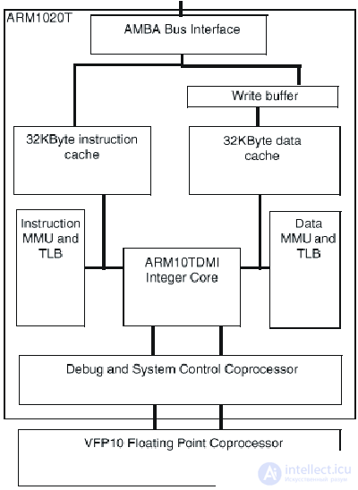
Рис.24.4. Блок-схема ядра ARM1020T
Главной особенностью семейства ARM10 является наличие векторного сопроцессора вычислений с плавающей точкой, явного свидетельства современной тенденции к объединению в одном приборе управляющих целочисленных процессоров и процессоров цифровой обработки сигналов..
В основе процессоров семейства ARM10 Thumb целочисленное ядро ARM10TDMI(TM), использующее ARM® 32-разрядную RISC систему команд, сжатую 16-разрядную систему команд Thumb и расширенные Multi-ICE средства отладки программного обеспечения. Ядро процессора ARM10TDMI - первая реализация ARMV5T Архитектуры Системы команд ( Instruction Set Architecture - ISA). Архитектура ARMV5T - некоторая комбинация архитектуры ARMV4 ISA, используемой StrongARM процессорами, и ARMV4T ISA используемой процессорами семейств ARM7 Thumb и ARM9 Thumb.
Ядро ARM10TDMI оснащено пятиуровневым конвейером, реализует параллельное выполнение команд, предсказание переходов и способно продолжать работу при неудачном обращении к кэш, обеспечивая высокую производительность в реальных применениях.
Уровни конвейера целочисленного процессора ARM10TDMI.
| F: | Выборка команды и предсказание перехода |
| D: | Декодирование команды и чтение регистра |
| E: | Выполнение (Сдвиг и ALU), вычисление адреса и умножение |
| M: | Обращение к памяти и умножение |
| W: | Запись в регистры |
Процессор ARM10T обеспечивает производительность 400 MIPS
( миллионов операций в секунду) на частоте 300 МГц, а векторное устройство операций с плавающей точкой, обеспечивает производительность 600 MFLOPS (миллионов операций с плавающей точкой в секунду). Такие уровни целочисленной и с плавающей точкой производительности необходимы для применений, оснащенных сложными интерфейсами с 2- и 3-мерной графикой, типа игровых видео плееров и высокопроизводительных принтеров, при сохранении доступных потребительских цен.
В настоящее время в семейство входит ARM1020T™ - кэшированное макроядро процессора, сформированное на основе ядра ARM10TDMI и оснащенное встроенными кэш команд и данных емкостью по 32 Кбайт, MMU, поддерживающим виртуальную память с подкачкой страниц по требованию, буфером записи, и широкополосным шинным интерфейсом AMBA, класса "система на кристалле".
Сопроцессор векторных вычислений с плавающей точкой VFP10 (Vector Floating Point - VFP) интегрируется на тот же кристалл что и процессор ARM1020T в тех применениях, для которых он необходим. Сопроцессор VFP10 - первая реализация новой архитектуры VFPV1 процессоров вычислений с плавающей точкой фирмы ARM. Сопроцессор VFP10 обеспечивает высокопроизводительные IEEE вычисления с плавающей точкой одиночной и двойной точности, занимая на кристалле площадь малого размера и при его реализации был использован RISC подход, заключающийся в том, что простые, наиболее часто используемые операции реализуются в кремнии (аппаратно) а для обработки редких исключительных случаев используются программные решения. Векторные операции хорошо использовать для обеспечения потребностей целевых применений и они обеспечивают существенный параллелизм при простой схемотехнике.
Векторный характер архитектуры VFP, с одним потоком команд и многими потоками данных (SIMD - single-instruction, multiple-data), позволяет одиночной команде оперировать с множеством элементов данных, что позволяет сразу выполнять многоадресные команды и существенно увеличивает производительность в применениях с интенсивными операциями с плавающей точкой.
В конвейере вычислений с плавающей точкой VFP10 используется два конвейера - пятиуровневый конвейер команд загрузки и памяти и семиуровневый конвейер арифметических команд. Эти конвейеры совместно используют два первых уровня, что ограничивает количество выполняемых команд одной командой, но из-за векторного характера архитектуры VFP в параллель могут быть выполнены команда векторной арифметики и векторной загрузки или команда сохранения.
The conveyor tracks five levels of loading and storage. In the case of multiple shipments, the pipeline memory level is used repeatedly for each data element. For each cycle two single precision values or one double precision value can be moved.
In a seven-level arithmetic pipeline, the first 3 levels correspond to the ARM pipeline, in which commands are received from ARM (sampling, decoding, and execution). The load and store commands and the data transfer commands remain committed to ARM for the next two cycles, in order to transfer data at the appropriate ARM memory level, and write data at the fifth level.
Low consumption of the ARM10 processor (less than 600 mW) allows devices with a high level of integration to be placed in low-cost housings, to use cheaper power components, which make it possible to abandon expensive means of heat dissipation.
Specialists from ARM set out the main ideas of the ARM10 processor family: in order to track the nature of work and, depending on this, reduce consumption, the developers abandoned the complexity and high cost of a fully superscalar machine. The required level of performance was achieved through the use of unique features of the ARM architecture, providing a high degree of internal parallelism in the once created machine. The command system of floating-point vector operations is completely new, so the developers, having analyzed the algorithms necessary for basic applications, had the opportunity to create a very fast device, using possible silicon solutions for the most frequently used operations, leaving the unique solutions to software solutions.
1. Characteristics of the RISC architecture.
2. The purpose of the mechanism of overlapping register windows.
3. Characteristic architecture of ARM.
4. Assigning a predicate to ARM.
5. Additional technologies in ARM.
6. Thumb and Thumb2 technologies.
7. Jazelle technology.
8. NEON technology.
9. VFP technology.
10. Security system TrustZone Technology.
11. Simplified architecture of the ARM7TDMI kernel.
12. Thumb decoding and decompression.
13. The block diagram of the core ARM1020T.
продолжение следует...
Часть 1 Theme 17. RISK - processors Lecture 24

Comments
To leave a comment
Computer circuitry and computer architecture
Terms: Computer circuitry and computer architecture