Lecture
In Section 12, the principles of the functioning of an elementary hypothetical microprocessor have already been considered (the term “microprocessor” and “processor” are further used as synonyms). Meanwhile, to study the principles of operation of even the simplest microcomputer, you must select a specific type of processor with a specific system of commands and control signals. An example of the simplest universal processor (i.e., a processor with a universal command system) of the battery type is the I8080 (the domestic equivalent of KR580VM80A), released by Intel in 1974. In the same year, the Altair 8800 computer was designed on the I8080 processor, which some experts call the first personal computer in the history of technology. It is this generation of 8-bit MPs (I8080, I8085, Z80, and others) that has become widely used in microcomputer controllers, control systems for industrial control systems, general-purpose microcomputers, and in office operations, mainly for word processing.
The I8080 processor has an 8-bit ALU and UU, made on a single chip, containing about 5000 transistors. BIS MP has 40 conclusions. The control device is made on the PLA and is not available to the user, i.e. The processor has a fixed instruction set. The supply voltage is ± 5 V and +12 V. The MP has two-phase synchronization (F 1 and F 2 ) at a clock frequency of up to 2.5 MHz and the following buses:
· ША - 16-bit. Used for addressing:
- RAM, ROM (R / W commands) - 16 bits (address space is 64 K);
- PU (I / O commands) - 8 bits (256 addresses);
· SD - 8-bit, bidirectional. Used by:
- to receive operands and commands from memory and PU;
- issuance of data (results) in memory and PU;
· SHU - not separately decorated and has 10 lines, through which 4 input and 6 output signals are transmitted.
The symbol of MP in the diagrams is shown in fig. 16.1.
Let us consider briefly, without detailed explanations, the assignment of control signals, given that a number of input and output signals form pairs, as it were, responsible for certain actions of the MP.
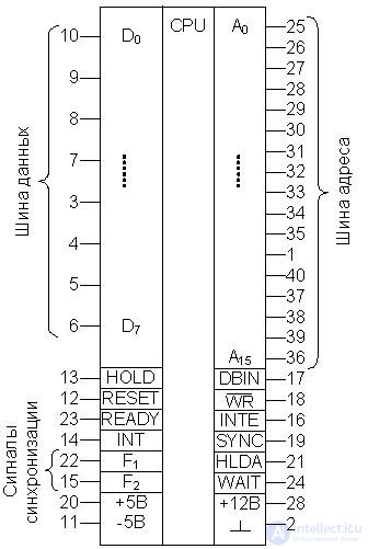
Fig.16.1. Symbol MP KP580VM80
Interrupt control
INT - input interrupt request signal from the control unit, perceived by the MP after the execution of the current command. The signal is not perceived if the MP is in the mode of capturing or disabling interrupts.
INTE - interrupt enable output. This signal reflects the state of the internal trigger "interrupt enable", which is set only by software.
Standby control
READY is an ready signal that signals the device's readiness to exchange with the MP. In its absence, the MP goes into standby state. Allows you to synchronize the work of MP and slower memory or PU. The READY signal can be set both from the control panel and from the auxiliary timer. In the simplest devices, this input is not used and is connected via a resistance to a +5 V source.
WAIT is an output waiting signal confirming that the MP is in standby mode.
Information Exchange Management
HOLD (HLD ) - input signal capture tires from PU. Translates buffers ША and ШД МП in the third state (state Z), i.e. MP is disconnected from the tire. This allows PU to occupy the trunk to initiate the exchange.
HLDA - output signal to confirm the state of the capture of MP.
Read / write control
DBIN - receive output signal. Indicates the memory and PU that the SM is in the mode of receiving information in the MP, i.e. in read mode.
 - output signal. Used to control the release of information from the MP to the memory and PU (recording mode). Is active
 = 0
= 0
Command counter management
RESET is a reset input. Sets to 0 the instruction address counter.
Synchronization
SYNC - sync output. Indicates the beginning of each new machine cycle.
F 1 , F 2 - synchro-sequence, determining the tact of the MP. Set by quartz generator.
A simplified functional diagram of the MP is shown in Fig. 16.2. The diagram shows only the functional connections between the main nodes of the MP. The transmission chains of control signals generating the corresponding micro-operations at the MP nodes are absent in the figure. The brackets indicate the capacity of the device MP.
Seven 8-bit registers are provided to store the data involved in the operation. PrGA, called a battery, is designed to exchange information with memory and PU, i.e. its contents can be issued to the SD or the number with the SD is written into it. When performing arithmetic, logical operations and shift operations, it serves as the source of the operand. It always contains the result of operations.
Six other registers are called B, C, D, E, H, L and form a block of general-purpose registers - RON. These registers are programmatically accessible and accessed by data transfer commands. Moreover, data exchange within the MP (ie, between RON, ALU and the battery) is carried out on the internal 8-bit bus via a bi-directional multiplexer. RON can store both data and addresses. These registers can be used in two ways - as single eight-bit registers and as register pairs BC, DE, HL for storing 16-bit binary numbers.
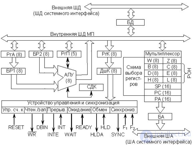
Fig.16.2. Functional diagram of MP
The registers BR1, BR2, W, Z are used as buffer and programmatically inaccessible (i.e., the user can not change their contents by means of commands).
The stack pointer SP is used to address stack memory and can store 16-bit addresses.
The PC command address counter is designed to store the 16-bit command address, or rather, the current byte address of the command, since commands can take 1, 2, 3 bytes. After sampling from the memory of the current byte, the contents of the counter are increased by 1, i.e. the next byte address is generated. When accessing memory (if indirect addressing is used), the contents of any register RON can be used as an address.
When issuing an address, the contents of the corresponding registers are transferred to a 16-bit address (PA) register, from which the address is then passed through the BA to the ShA of the system interface.
MP has an 8-bit ALU, which allows you to perform 4 arithmetic operations (addition with transfer and transfer to the lower category and without it, subtraction with transfer of the loan to the lower category and without it), four types of logical operations (conjunction disjunction, inequality, comparison), as well as 4 types of cyclic shifts.
When performing arithmetic operations one of the operands is always the contents of the battery. The result is always placed in the battery. Cyclic shift is performed only on the contents of the battery.
It is possible to perform arithmetic operations on decimal numbers. In this case, two decimal digits in the code 8421 are placed in a byte. When considering the operations of decimal arithmetic, it was noted that a correction of the result may be necessary, i.e. adding to it the number 0110 (2) . Such a correction in each tetrade of the result is carried out by a decimal correction circuit (KFOR).
Earlier it was noted that the RSL is also called the register of flags and often denoted by the letters F or F. This is an 8-bit register in which only 5 bits are used. It is intended to store a number of features detected in a number that is the result of an operation in an ALU or RON. Register triggers have the following purpose:
T c (transfer trigger) - set to 1 if there is a transfer from the high-order bit when performing arithmetic operations (c = 1 - there is a transfer; c = 0 - there is no transfer). In addition, it remembers the contents of the discharge that is being pushed out of the battery when performing a shift operation.
T z (zero trigger) is set to the logical state 1 if the result of an operation in an ALU or an operation of incrementing the RON content is 0 (z = 1 - the result is 0, z = 0 - the result is not 0).
T s (sign trigger) is set to the state corresponding to the high-order value of the result of the operation in the ALU or the operation of incrementing the RON content (s = 0 - the result is positive, s = 1 - the result is negative).
T p (parity trigger) - is set to the logical state 1, if the number of ones in the bits of the result is even (p = 1 - the weight of the result is even, p = 0 is odd).
T v (trigger additional transfer) stores the transfer from the 3rd category, arising from the operation in the ALU.
It consists of the command register, where the first byte of the command is received, the command decoder and the control device itself, which generates control signals, under the action of which micro-ops sequences are executed in individual MP nodes. As already noted, the control device is made on the PLA, i.e. Firmware is stored at the expense of a hard link system and cannot be changed by the user. Four input and six output signals of the control device in the presence of a system controller allow the processor to control computing systems of a rather complex structure.
Address and data buffers link MPs with external address and data buses (system interface buses). Buffers use three-state logic elements as output stages. This allows the processor to disconnect from external buses and make them available to the CPU. The SD buffer is bidirectional, which allows using the SD in half-duplex mode for receiving and transmitting information in non-overlapping time intervals.
The principle of bidirectional data exchange between the internal and external SM can be explained by the scheme shown in Fig. 16.3.
It should be remembered that the transmission of information on buses, both internal and external, is carried out in parallel code, i.e. output and input logic elements of the SD buffer have an 8-channel structure.
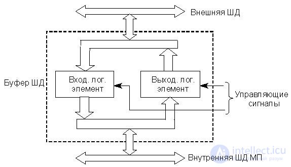
Fig.16.3. Functional diagram of the buffer SD MP
From the user's point of view, the implementation of the physical processes occurring in the microcircuit is of no particular interest, as is the physical implementation of individual MP nodes. The user is provided with a number of formal MP devices with which he can perform various manipulations through program commands. To communicate with a device, the user needs to know the address or number of this device.
The structure of the MP I8080 (KR580), from the point of view of the programmer, is presented in Fig. 16.4. The battery and the register of features (flags) are the halves of one 16-bit register, but the user can access them as separate 8-bit registers. In the documentation for MP KR580, the contents of the RGP are called the processor status word (PSW). However, some authors by PSW understand not only the contents of the PRP, but also the contents of the battery, i.e. PSW (A) (F). This interpretation of the PSW (PSW register) is used in the further presentation of the material.
Thus, the user has at his disposal:
- eight-bit registers A, B, C, D, E, H, L, each of which has its own three-digit address (number);
- 16-bit register pairs BC, DE, HL, defined by the name of the highest register of the pair (ie, B, D, H);
- 16-bit registers PC, SP, PSW;
- 8-bit RSB (F), which can be considered separately from the PSW;
- one-bit register (trigger) enable interrupts.

Fig.16.4. MP from the point of view of the programmer
In more detail РгП (F) is represented in fig. 16.5.
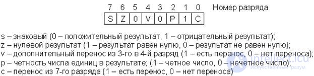
Fig.16.5. Register of signs
The main data format is shown in Fig. 16.6.

Fig.16.6. Basic data format
In a microprocessor, a data byte can be interpreted as follows:
· Unsigned integer
255 (10) = 1111 1111 (2) = FF (16) (FFH)
. . . . . . . . . . . . . . . .
0 (10) = 0000 0000 (2) = 00 (16) (00H).
· Signed number in additional code
+127 (10) = 0111 1111 (2) = 7F (16)
. . . . . . . . . . . . . . . .
0 (10) = 0000 0000 (2) = 00 (16)
-1 (10) = 1111 1111 (2) = FF (16)
. . . . . . . . . . . . . . . .
-128 (10) = 1000 0000 (2) = 80 (16) .
· Two-digit binary decimal
99 (10) = 1001 1001 (2) = 99 (16)
. . . . . . . . . . . . . . . .
0 (10) = 0000 0000 (2) = 00 (16) .
· The logical data byte.
In some cases, a two-byte data format is used:
· Double-byte signed number in additional code

· Unsigned two-byte number

For commands, one-, two-, three-byte formats are used, and the operation code (CPC) always takes 1 byte. In addition, it should be remembered that the SHA has 16 discharges, i.e. allows you to address memory in 64K single-byte cells. Therefore, in this case, the address requires 2 bytes.
At the same time, using the INPUT / OUTPUT commands, the programmer can address the 256 registers of the foam. Consequently, in this case only 1 byte is required for the address, which is transmitted according to the low-order bits of the AE 7 ... A 0 . (The same byte is duplicated in the high-order bits of AAS 15 ... A 8 , that is, if the address of the register is F8, then F8F8 is present on the AC).
In general, the formats of MP commands are of the form shown in Fig. 16.7. The first byte contains the CPC, and the second one contains the single-byte operand or the number of the FPU register (fig. 16.7, a, b).
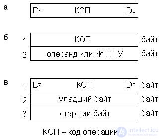
Fig.16.7. Command Formats
In a three-byte format (Fig. 16.7, c), the first byte contains the operation code (CPC). The next two bytes contain, respectively, the low and high bytes of the address of the OP cells (ROM) or a two-byte operand.
We will consider the addressing methods very briefly, since all types of addressing in a general form have been analyzed previously.
Direct addressing
In this case, the source or receiver of the operand are memory cells or the FPU register.
The address of the memory cell or register PUF is recorded in the command:
- two-byte command - address of the PPU register;
- three-byte command — memory address.
Register Addressing
In this case, the source or receiver of the operand is RON. RON number is recorded in the operation code. Single -byte commands (RON number - 3 digits).
Indirect addressing
In this case, the source or destination of the operand is a memory cell. Commands are single-byte . The address of the memory cell is in the register pair, for example HL. There are increment and decrement commands (± 1) of the contents of the register pairs, which allows you to modify the address.
Stack addressing
In this case, the source or destination of the operand is a memory cell. Commands are single-byte .
The address of the top of the stack is in the SP stack pointer. When filled, the stack grows towards decreasing addresses, i.e. a stack is formed, which was previously called inverted. The start address of the stack is set in the stack pointer (SP) programmatically. It has already been noted that SP has 16 bits, so if the initial address of the stack is to choose the last address of the entire address space, then the stack can have a capacity of 64 KB.
The exchange with the stack (i.e. loading / unloading) is performed with two-byte words. In this case, loading into the stack is reduced to the following sequence of actions by the MP:
- operation is performed (SP) = (SP) - 1;
- at the new address the high byte of the entered two-byte is written
the words;
- operation is performed (SP) = (SP) - 1;
- the low byte (second) of the entered two-byte word is written to the new address.
Unloading the stack is as follows:
- reads the low byte at (SP);
- the operation is performed (SP) = (SP) + 1;
- read high byte at the new address;
- the operation is performed (SP) = (SP) + 1.
Direct Addressing
In this case, the operand is in the command itself. The operand can be one- and two-byte. Accordingly, commands can be double-byte and three-byte (the first byte always occupies the CPC).
It should be remembered that in a three-byte command, the lower bits of the 16-bit number are contained in the second byte of the command, and the oldest in the third.
1. Give the symbol MT KP580VM80. Describe the purpose of all the findings.
2. Functional diagram of MP KR580VM80.
3. Assignment of individual bits of the status word of the register of attributes MP KR580VM80.
4. Functional diagram of the buffer SD MP KP580VM80.
5. MP KR580VM80 from the point of view of the programmer.
6. Formats of data and commands in MP KR580VM80.
7. Addressing methods in MP KR580VM80.

Comments
To leave a comment
Computer circuitry and computer architecture
Terms: Computer circuitry and computer architecture