Lecture
In the previous sections, the simplest digital electronic components that perform fixed logic functions, the so-called “loose logic”, were studied. Their study allows us to proceed to the consideration of more complex components, in which from tens of units to hundreds of millions of simple elements are integrated. These include:
- programmable logic devices (PLD),
- programmable logic integrated circuits (FPGAs),
- Custom Integrated Circuits (ASIC - application specific integrated circuit)
The smallest degree of integration differs PLD, which are used to solve small and fairly simple tasks. They can be configured (reprogrammed) by the user to implement various functions. Unlike them, custom ASIC integrated circuits can contain hundreds of millions of simplest logic elements (gates) and can perform very complex functions. Their development is a complex, lengthy and expensive process, which is engaged in large specialized companies. Therefore, it is advisable for external consumers to consider only their architecture and interaction with the external environment enlarged, without going into details of the circuit design of individual nodes. The basics of computer architecture implemented in the form of ASIC will be discussed in the following sections.
FPGAs occupy an intermediate position between PLD and custom integrated circuits. On the one hand, the functions they implement can be promptly programmed and reprogrammed in place by the user. On the other hand, FPGAs can contain millions of logic gates, which makes it possible to implement extremely large and complex functions.
Figure 6.1 shows an example of a simple programmable function with two inputs a and b and one output y.
In the presence of jumpers to the inputs of the coincidence circuit (operation AND) input signals can be fed in direct and inverse form. In the absence of any jumper, the logical input 1 is supplied to the corresponding input of the coincidence circuit via the load resistor. Different programming methods differ in the physical principles of jumper setting.
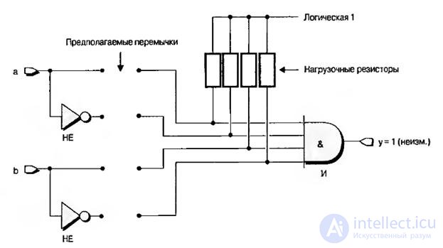
Fig.6.1. Simple programmable function
When using the fusible jumper method, the device is manufactured with all the jumpers (Fig.6.2), which the developer can selectively remove (burn) by applying to the device inputs pulses of relatively high voltage and high current. If, for example, the F af and F bt jumpers are removed from the circuit in Fig. 6.2 (Fig. 6.3), then the device will form the function

The process of removing jumpers is called the programming process (burning) of the device. Devices whose configuration is based on the fused jumper method are once programmable devices, since after burning the fused jumper cannot be restored.
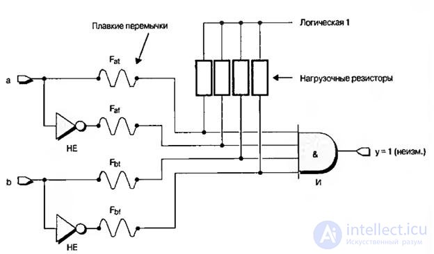
Fig.6.2. Filling the device with unprogrammed fusible jumpers

Fig.6.3. Fusible jumpers after programming
This method is directly opposite to the fusible jumper method. In the unprogrammed state, all jumpers are present in the device, but they have such a high resistance that they can be considered as an open circuit. The expandable bridge is initially a microscopic column of amorphous (non-crystalline) silicon connecting two metal conductors. Jumper extension (programming) is carried out by converting the amorphous silicon-insulator into conductive polycrystalline silicon using impulses of relatively high voltage and high current applied to the device inputs. For example, if jumpers are built up in the circuit of inverted input a and direct input b, the device will realize the function (Fig. 6.4)


Fig.6.4. Stackable jumpers after programming
Once grown jumper can not be destroyed or returned to its original state. Therefore, devices whose configuration is based on the method of expandable jumpers are once programmable.
Photomasks are used to create transistors and metal conductors connecting them on a silicon crystal, which are called metallization layers, and the programming process is also called mask programming. Consider, for example, a transistor cell of a persistent storage device (ROM) that can store one data bit (Figure 6.5). 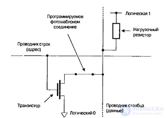
Fig.6.5. Transistor Cell ROM, programmable photomask
A standard ROM device consists of a number of lines.
(addresses) and columns (data), which together form an array of data. One load resistor is connected to each column, which allows you to maintain a logic unit level at the column output, and at each intersection of the row and column there is a transistor and, if necessary, a jumper. The presence / absence of the jumper is set by the photomask. Programming the ROM using an individually made template is that it uses cells with jumpers and cells without jumpers.
When the active signal is applied to the conductor of the line, all transistors connected to it are transferred to the open state. In the case when a cell contains a connection programmed using a photomask, the open transistor of this cell will connect the column conductor with a logic level of 0. Conversely, if there is no programmed connection in the cell, the transistor will not make any action through the load resistor connected to the column , the output of the chip will receive a logic level of 1.
Mask programming is used to program ROMs and implement simple logic functions in the form of truth tables.
The disadvantage of devices programmed by a photomask is the high unit cost of production with a small circulation and the inconvenience of using if necessary to frequently change the configuration of components.
Unlike once programmed devices, in practice it is often more convenient to deal with repeatedly programmable devices.
(reprogrammed) devices. One option is to use erasable programmable read-only memory (EPROM).
The EPROM transistor has the same structure as a standard MOSFET, but with an additional (second) floating gate made of polycrystalline silicon, insulated with silicon oxide layers. In the unprogrammed state, the floating gate is not charged and does not affect the operation of the normal gate. In order to program the transistor, it is necessary to apply a relatively high voltage, about 12 volts, to the gate contacts. In this case, the transistor turns on abruptly, and fast electrons overcome the layer of silicon oxide, heading for the floating gate. After removing the programming signal, the negatively charged particles remain in the floating gate. Their charge is stable and, subject to the rules of operation, does not dissipate for more than 10 years. Charges accumulated on a floating gate block the normal operation of a normal shutter and, thus, make it possible to distinguish the programmed cells from the unprogrammed ones. Due to this property, such transistors can be used to form memory cells (Fig.6.6).
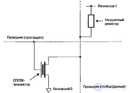
Fig.6.6. Memory cell based on EPROM transistor
Such a memory cell no longer needs fused jumpers, stackable jumpers, or photo-programmable connections. For programming, the device inputs are used to charge the floating gates of selected transistors, thereby blocking their operation. In these cases, logical 1 cells will be stored in the memory cells. Erasing the memory cells is nothing but the “leakage” of electrons from the floating gate, which occurs under the influence of ultraviolet radiation.
The next step of the technological ladder was an electrically erasable programmable read-only memory (EEPROM). Unlike the EPROM cell, the EEPROM cell contains two transistors, the first of which is identical to the EPROM transistor, but has a very thin insulating layer of silicon oxide around the floating gate. The second transistor is used to erase the memory cell electrically.
The technology, known as Flash, is similar to EEPROM. However, due to the architectural features of the organization, individual cells cannot be erased, but only the entire device, or in large parts.
The definition of “static” in the name of a static random access memory (RAM) reflects the fact that once the value recorded in the memory cell will remain in it until it is specifically changed or the system is de-energized. The designation of a memory cell based on static RAM is shown in Fig.6.7.
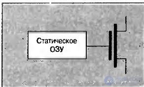
Fig.6.7. Programmable memory cell based on static RAM
The memory cell contains a multi-transistor element of static RAM, the output of which is connected to an additional control transistor. Depending on the content (logical 0 or logical 1) of the memory element, the control transistor will be closed (that is, turned off) or open (that is, turned on). One of the drawbacks of programmable devices based on static RAM memory cells is that each cell occupies a significant area on the surface of a silicon crystal, since it consists of four or six transistors configured as a register latch (registers triggered by level). Another disadvantage is that device configuration data will be lost when the power is turned off. At power up, device configuration will need to be done again. The main advantage of using memory cells based on static RAM is the ability to quickly and reprogram the device infinitely many times.
Table 6.1 briefly lists the most important characteristics of the considered design technologies regarding their use in the FPGA. The EPROM technology absent in the table is not used in the FPGA.
Table 6.1. Characteristics of programming technology
| Characteristic | Static RAM | Stackable jumpers | EEPROM / Flash |
| Technological process | Modern level of development | Lagging for one or several generations | Lagging for one or several generations |
| Reprogramming | Yes (intra-systemic) | Not | Yes (internal or disabled) |
| Speed reprogramming (including erasing) | Fast | - | 3 times slower than static RAM |
| Volatility (possibility of programming at power up) | Yes | Not | No (possible if necessary) |
| The need for an external configuration file | Yes | Not | Not |
| Suitability for prototyping devices | Yes (high availability) | Not | Yes (acceptable) |
| Ready to work immediately after power on | Not | Yes | Yes |
| Intellectual Property Protection | Acceptable | Very good | Very good |
| Configuration Cell Size | Large (six transistors) | Very small | Small (two transistors) |
| Power consumption | Average | Low | Average |
| Radiation resistance | Not | Yes | Not |
Programmable logic devices (PLU) are conventionally divided into simple PLD (SPLD - simple programmable logic devices) and complex PLD (CPLD - complex progmmable logic devices), which, in turn, are divided into versions depending on the programming technologies used (Fig. 6.8) .
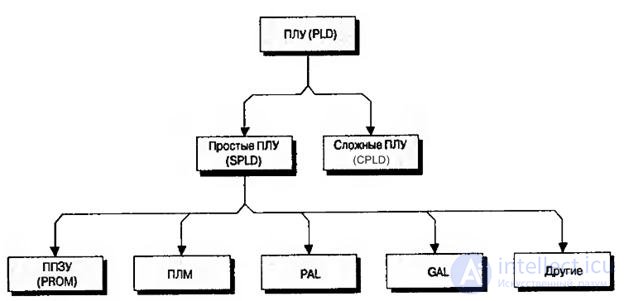
Fig.6.8. An abundance of PLU architectures
In the previous sections, the simplest digital electronic components that perform fixed logic functions, the so-called “loose logic”, were studied. Their study allows us to proceed to the consideration of more complex components, in which from tens of units to hundreds of millions of simple elements are integrated. These include:
- programmable logic devices (PLD),
- programmable logic integrated circuits (FPGAs),
- Custom Integrated Circuits (ASIC - application specific integrated circuit)
The smallest degree of integration differs PLD, which are used to solve small and fairly simple tasks. They can be configured (reprogrammed) by the user to implement various functions. Unlike them, custom ASIC integrated circuits can contain hundreds of millions of simplest logic elements (gates) and can perform very complex functions. Their development is a complex, lengthy and expensive process, which is engaged in large specialized companies. Therefore, it is advisable for external consumers to consider only their architecture and interaction with the external environment enlarged, without going into details of the circuit design of individual nodes. The basics of computer architecture implemented in the form of ASIC will be discussed in the following sections.
FPGAs occupy an intermediate position between PLD and custom integrated circuits. On the one hand, the functions they implement can be promptly programmed and reprogrammed in place by the user. On the other hand, FPGAs can contain millions of logic gates, which makes it possible to implement extremely large and complex functions.
Figure 6.1 shows an example of a simple programmable function with two inputs a and b and one output y.
In the presence of jumpers to the inputs of the coincidence circuit (operation AND) input signals can be fed in direct and inverse form. In the absence of any jumper, the logical input 1 is supplied to the corresponding input of the coincidence circuit via the load resistor. Different programming methods differ in the physical principles of jumper setting.
Fig.6.1. Simple programmable function
When using the fusible jumper method, the device is manufactured with all the jumpers (Fig.6.2), which the developer can selectively remove (burn) by applying to the device inputs pulses of relatively high voltage and high current. If, for example, the F af and F bt jumpers are removed from the circuit in Fig. 6.2 (Fig. 6.3), then the device will form the function
The process of removing jumpers is called the programming process (burning) of the device. Devices whose configuration is based on the fused jumper method are once programmable devices, since after burning the fused jumper cannot be restored.
Fig.6.2. Filling the device with unprogrammed fusible jumpers
Fig.6.3. Fusible jumpers after programming
This method is directly opposite to the fusible jumper method. In the unprogrammed state, all jumpers are present in the device, but they have such a high resistance that they can be considered as an open circuit. Наращиваемая перемычка первоначально представляет собой микроскопический столбец аморфного ( некристаллического) кремния, связывающего два металлических проводника. Наращивание перемычки ( программирование) осуществляется путём преобразования аморфного кремния-изолятора в токопроводящий поликристаллический кремний с помощью подаваемых на входы устройства импульсов относительно высокого напряжения и большого тока. Например, если нарастить перемычки в цепи инвертированного входа a и прямого входа b, то устройство будет реализовывать функцию ( рис.6.4)
Рис.6.4. Наращиваемые перемычки после программирования
Однажды выращенная перемычка не может быть разрушена или возвращена в исходное состояние. Поэтому устройства, конфигурирование которых основано на методе наращиваемых перемычек являются однократно программируемыми.
Фотошаблоны используются для создания транзисторов и соединяющих их на кремниевом кристалле металлических проводников, которые называются слоями металлизации, а сам процесс программирования ещё называют масочным программированием. Рассмотрим, например, транзисторную ячейку постоянного запоминающего устройства (ПЗУ), которая может хранить один бит данных ( рис. 6.5).
Рис.6.5. Транзисторная ячейка ПЗУ, программируемая фотошаблоном
Стандартное устройство ПЗУ состоит из некоторого количества строк
( адреса) и столбцов ( данные), которые вместе образуют массив данных. К каждому столбцу подключен один нагрузочный резистор, который позволяет поддерживать на выводе столбца уровень логической единицы, а в каждом пересечении строки и столбца присутствует транзистор и, при необходимости, перемычка. Наличие/отсутствие перемычки задаётся фотошаблоном. Программирование ПЗУ с помощью индивидуально изготовленного шаблона состоит в том, что с его помощью определяются ячейки с перемычками и ячейки без перемычек.
При подаче активного сигнала на проводник строки все, подключённые к ней транзисторы, переводятся в открытое состояние. В случае, когда ячейка содержит запрограммированное по фотошаблону соединение, открытый транзистор этой ячейки будет соединять проводник столбца с уровнем логического 0. И наоборот, если в ячейке нет запрограммированного соединения, транзистор не будет вносить какого-либо действия и через нагрузочный резистор, подсоединённый к столбцу, на выход микросхемы будет поступать уровень логической 1.
Масочное программирование используется для программирования ПЗУ и реализации простых логических функций в виде таблиц истинности.
Недостатком устройств, программируемых фотошаблоном, является высокая удельная стоимость производства при малом тираже и неудобство использования при необходимости часто менять конфигурацию компонентов.
Unlike once programmed devices, in practice it is often more convenient to deal with repeatedly programmable devices.
(reprogrammed) devices. One option is to use erasable programmable read-only memory (EPROM).
СППЗУ-транзистор имеет такую же структуру, как стандартный МОП-транзистор, но с дополнительным ( вторым) плавающим затвором из поликристаллического кремния, изолированного слоями оксида кремния. В незапрограммированном состоянии плавающий затвор не заряжен и не влияет на работу обычного затвора. Чтобы запрограммировать транзистор, необходимо приложить к контактам затвора относительно высокое напряжение, около 12 Вольт. При этом транзистор резко включается, и быстрые электроны преодолевают слой оксида кремния, направляясь в плавающий затвор. После снятия сигнала программирования, отрицательно заряженные частицы остаются в плавающем затворе. Их заряд стабилен и при соблюдении правил эксплуатации не рассеивается на протяжении более 10 лет. Накопленные на плавающем затворе заряды блокируют нормальную работу обычного затвора и, таким образом, позволяют отличать запрограммированные ячейки от незапрограммированных. Благодаря этому свойству такие транзисторы можно использовать для формирования ячеек памяти (рис.6.6).
Рис.6.6. Ячейка памяти на основе СППЗУ-транзистора
Такая ячейка памяти больше не нуждается в плавких перемычках, наращиваемых перемычках или программируемых фотошаблоном соединениях. Для программирования используются входы устройства для заряда плавающих затворов выбранных транзисторов, тем самым блокируя их работу. В этих случаях в ячейках памяти будут храниться логические 1. Стирание ячеек памяти есть не что иное, как ”вытекание” электронов из плавающего затвора, которое происходит под воздействием ультрафиолетового излучения.
Следующая ступенька технологической лестницы представляла собой электрически стираемое программируемое постоянное запоминающее устройство (ЭСППЗУ). В отличие от ячейки СППЗУ, ячейка ЭСППЗУ содержит два транзистора, первый из которых идентичен СППЗУ-транзистору, но имеет очень тонкий изолирующий слой оксида кремния вокруг плавающего затвора. Второй транзистор используется для стирания ячейки памяти электрическим способом.
Технология, известная как Flash, аналогична ЭСППЗУ. Однако, в связи с архитектурными особенностями организации, отдельные ячейки не могут стираться, а только всё устройство целиком, либо большими частями.
Определение ”статическое” в названии статического оперативного запоминающего устройства (ОЗУ) отражает тот факт, что однажды записанное в ячейку памяти значение будет оставаться в ней неизменным до тех пор, пока не будет специально изменено или система не будет обесточена. Обозначение ячейки памяти на основе статического ОЗУ приведено на рис.6.7.
Рис.6.7. Программируемая ячейка памяти на основе статического ОЗУ
Ячейка памяти содержит мультитранзисторный элемент статического ОЗУ, выход которого подключён к дополнительному управляющему транзистору. В зависимости от содержимого ( логический 0 или логическая 1) элемента памяти управляющий транзистор будет закрыт ( то есть отключен) или открыт ( то есть включён). Один из недостатков программируемых устройств на основе ячеек памяти статического ОЗУ состоит в том, что каждая ячейка занимает значительную площадь на поверхности кремниевого кристалла, так как состоит из четырёх или шести транзисторов, сконфигурированных в виде регистра-защёлки ( регистры, срабатывающие по уровню). Другим недостатком является то, что данные о конфигурации устройства будут утеряны при отключении питания. При включении питания конфигурирование устройства необходимо будет делать заново. Основным достоинством использования ячеек памяти на основе статического ОЗУ является возможность быстро и бесконечное число раз перепрограммировать устройство.
В таблице 6.1 кратко перечислены наиболее важные характеристики рассмотренных технологий проектирования относительно их использования в ПЛИС. Отсутствующая в таблице технология СППЗУ в ПЛИС не используется.
Таблица 6.1. Характеристики технологий программирования
| Characteristic | Статическое ОЗУ | Наращиваемые перемычки | ЭСППЗУ/Flash |
| Технологический процесс | Современ-ный уровень развития | Отставание на од-но или несколько поколений | Отставание на од-но или несколько поколений |
| Reprogramming | Да( внутри-системно) | Not | Да( внутрисистем-но или в выклю-ченном состоянии) |
| Скорость перепрограммиро-вания ( включая стирание) | Fast | - | В 3 раза медленнее статического ОЗУ |
| Энергозависимость (возмож-ность программирования при включении питания) | Yes | Not | Нет ( возможно при необходимости) |
| Потребность во внешнем конфигурационном файле | Yes | Not | Not |
| Пригодность для изготовления прототипов устройств | Да ( высокая пригодность) | Not | Да ( приемлемо) |
| Готовность к работе сразу после включения питания | Not | Yes | Yes |
| Защита прав интеллек-туальной собственности | Acceptable | Очень хорошая | Очень хорошая |
| Размер конфигурационной ячейки | Большой ( шесть тран-зисторов) | Очень малый | Малый ( два транзистора) |
| Мощность потребления | Average | Low | Average |
| Устойчивость к радиации | Not | Yes | Not |
Программируемые логические устройства (ПЛУ) условно подразделяют на простые ПЛУ ( SPLD – simple programmable logic devices) и сложные ПЛУ (CPLD – complex progmmable logic devices), которые, в свою очередь делятся на разновидности в зависимости от используемых технологий программирования ( рис.6.8).
Рис.6.8. Изобилие архитектур ПЛУ
Для примера на рис.6.12 приведена незапрограммированная ПЛМ на три входа и три выхода, а на рис.6.13 показана запрограммированная ПЛМ, реализующая следующие три уравнения :

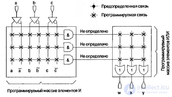
Рис.6.12. Незапрограммированная ПЛМ
Наряду с преимуществами, которые имеют ПЛМ по сравнению с ППЗУ, у них есть и недостатки. Сигналам для прохождения через программируемые связи требуется больше времени, чем через предопределённые аналоги. Поэтому ПЛМ работает медленнее, чем ППЗУ, так как оба массива и функций И и функций ИЛИ являются программируемыми.

Рис.6.13. Запрограммированная ПЛМ
Для того, чтобы решить проблему быстродействия, свойственную ПЛМ, в конце 1970-х появился новый класс устройств, называемый программируемый массив логики (ПМЛ или PAL – Programmable Array Logic). В отличие от ППЗУ они состоят из программируемого массива логических функций И и предопределённого массива функций ИЛИ. Устройства GAL ( Generic Array Logic – изменяемый массив логики), разработанные в 1983 году компанией Lattice Semiconductor Corporation, представляют собой более сложные электрически стираемые КМОП-разновидности идеологии PAL.
В качестве примера на рис.6.14 приведено простое PAL-устройство с тремя входами и тремя выходами. Преимуществом микросхем PAL по сравнению с ПЛМ является более высокое быстродействие, так как из двух массивов у них только один является программируемым.
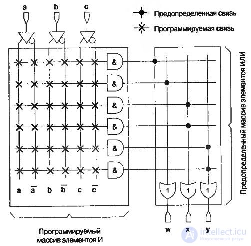
Рис.6.14. Незапрограммированное устройство PAL
В отличие от рассмотренных выше примеров микросхем ПЛМ и PAL, промышленность выпускает очень большие ПЛМ и PAL с множеством входов, выходов и с внутренними сигналами. В них могут быть предусмотрены дополнительные программируемые опции, такие, как возможность инвертировать выходы, либо иметь выходы с тремя состояниями, либо и то и другое. Кроме того, некоторые из них поддерживают регистровые выходы и позволят пользователю выбрать версию выхода – регистровую или нерегистровую. Некоторые устройства позволяют конфигурировать определённые выводы в качестве либо выходов, либо дополнительных входов. Этим списком не ограничивается список дополнительных опций, который постоянно пополняется разными производителями.
В начале 1980-х были разработаны более сложные программируемые логические устройства, так называемые сложные ПЛУ (CPLD – complex PLD). Они отличались от простых ПЛУ большей функциональностью, меньшими физическими размерами, более высоким быстродействием и меньшей стоимостью.
Существенный технологический прорыв в этом направлении совершила компания Altera, которая представила сложное ПЛУ, основанное на сочетании КМОП- и СППЗУ-технологий., и в котором использовался центральный коммутационный массив с количеством соединений с входами/выходами блоков менее 100%. Это осложнило программное обеспечение для проектирования ПЛУ, но позволило существенно увеличить быстродействие и значительно снизить потребляемую мощность и стоимость этих устройств.
Несмотря на то, что каждый производитель сложных ПЛУ реализовывал свои уникальные технологии, в общем случае устройство состояло из нескольких блоков простыл ПЛУ, обычно PAL, объединённых общей программируемой коммутационной матрицей ( рис.6.15). Помимо отдельных блоков простых ПЛУ можно было также запрограммировать соединения между ними с помощью программируемой коммутационной матрицы.
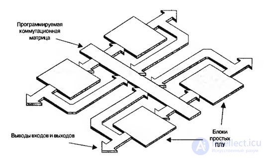
Рис.6.15. Общая структура сложного ПЛУ
На рис.6.15 не показаны различные дополнительные компоненты и он даёт лишь поверхностное представление о работе сложного ПЛУ. Все структуры сформированы на одном кристалле кремния. Например, программируемая коммутационная матрица может содержать большое количество проводников, скажем 100. Но это больше, чем может быть подключено к блоку простого ПЛУ, который способен работать только с ограниченным количеством сигналов, скажем 30. Блоки простых ПЛУ связаны с коммутационной матрицей своего рода программируемыми мультиплексорами ( рис.6.16).
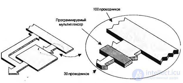
Рис.6.16. Использование программируемых мультиплексоров
В зависимости от производителя и от типа устройства программируемые переключатели сложных ПЛУ могут быть выполнены на ячейках памяти типа СППЗУ, ЭСППЗУ, Flash или на статическом ОЗУ. При использовании статического ОЗУ появляется возможность увеличить универсальность этой памяти, используя её в качестве программируемых переключателей и в качестве фактической оперативной памяти.
1. Дайте пример простой программируемой функции.
2. Опишите метод плавких перемычек.
3. Опишите метод наращиваемых перемычек.
4. Принцип программирования устройств фотошаблоном.
5. Опишите ячейку памяти на основе СППЗУ-транзистора.
6. Нарисуйте примеры незапрограммированной и запрограммированной схем ППЗУ.
7. Нарисуйте примеры незапрограммированной и запрограммированной схем ПЛМ.

Comments
To leave a comment
Computer circuitry and computer architecture
Terms: Computer circuitry and computer architecture