Lecture
Earlier, when considering the generalized structure of a computer, it was noted that the main device directly involved in processing the information supplied to a computer is a processor (in large computers it is a central processor). Naturally, specific types of computers contain in their composition processors built according to different schemes, and processors of large computers differ significantly from mini- and microcomputers (there is no reason to talk about supercomputers). However, the basic principles of the construction of processors are, in general, the same, and most clearly they can be demonstrated by the example of the simplest hypothetical microprocessor.
Previously, actions on numbers (addition, subtraction, multiplication), presented in various forms, were considered. It was emphasized that all these actions are carried out using elementary operations that are performed in a certain sequence .
These elementary operations include:
- write the number to the register;
- inverting the contents of the register bits;
- forwarding the contents of the registers;
- shift the contents of the register;
- addition of codes;
- bitwise logical operations or bit analysis;
- account operation with + 1 or s-1 (increment or decrement).
Example.
The multiplication operation is implemented using:
- analysis of the discharge factor;
- summation;
- shift.
All these actions are performed in a device called a processor, which consists of two devices - an operating unit (OU) and a manager (UU).
OU - performs the specified elementary operations.
CU - controls the OS, setting the necessary sequence for performing these operations.
This is consistent with the principle of V.M. Glushkov, that in any digital information processing device, it is possible to distinguish operational and control units.
As the nodes of the SU and the OS include registers, counters, adders, multiplexers, decoders, etc., i.e. pulse digital devices. In addition, the normal functioning of the processor and the entire computer is possible only in the presence of highly stable pulse sequences, formed, as a rule, from a single pulse sequence produced by a quartz oscillator. These clock pulse sequences synchronize the operation of processor nodes, and sometimes the entire computer.
The generalized structure of any processor is shown in Fig. 15.1.

Fig.15.1. Generalized processor structure
Each elementary operation performed in one of the OS nodes during one clock period is called a micro-operation .
During certain clock periods, several micro-operations can be performed simultaneously, for example: R 2 ¬ 0, MF ¬ (MF) - 1, etc. Such a set of consistent microoperations is called a microinstruction , and a set of microinstructions designed to solve a problem is called a microprogram .
If the OS provides for the possibility of performing n different micro-operations, then the control unit must have n control circuits S 1 , ..., S n , each of which corresponds to its micro-operation. Due to the fact that the CU determines the firmware, i.e. what and in what time sequence micro-operations should be performed, it is called the microprogram automaton . Accordingly, OU is often called an operating machine .
The formation of control signals S 1 , ..., S n may depend both on external signals of the CPC (assembler commands) and on the state of the OS nodes determined by the communication signals of the status signs P 1 , ..., P m coming from the output of the OS to the corresponding inputs of the SU.
As already noted, OU performs various arithmetic and logical operations on the source data; therefore, OU is most often called the arithmetic logic unit, or ALU.
The division of any processor into software and operating machines is quite obvious and does not cause any special difficulties in understanding. However, the structural schemes of even the simplest real processors, in addition to the ALU and the SU, also contain a number of nodes (registers, counters, decoders), which do not seem to relate to the ALU or the SU. To eliminate confusion in the following material, a number of observations must be made:
1. In the absolute majority of cases, digital information processing devices have a multi-level structure, i.e. built on the principle of "matryoshka". This means that the SU and the DU may themselves break up into pairs of the SU 'and the DU', which, in turn, may also break up into the corresponding SU and the DU. It all depends on the degree of detail the review of this digital device. This principle of multilevel is valid for all computer devices.
Indeed, if we consider the processor as a whole and divide it into CU and OU, then it makes absolutely no difference how arithmetic-logic operations are performed at the OS - using very complex logic circuits or using simple logic that runs under the control of some auxiliary CU. Similar reasoning is true for CU.
So, for example, the central processor of large general-purpose computers of the mid-70s was divided into 4-5 levels, each of which can be distinguished with its own SU and OU. Modern processors have an even more complex structure.
Moreover, these considerations are true in general for computers, which can be decomposed into a number of virtual (seeming) machines and each one works at an appropriate level. In the general case, modern universal computers have six levels:
-  level of problem-oriented language;
- procedural language;
- assembly level (assembly language);
- operating system level (language of the operating system);
-  traditional machine level (machine command language);
- microprogram level (language of microinstructions).
The machine languages of the two lower levels are digital, and the programs on them consist of long numerical sequences that are very inconvenient for humans, but understandable to the machine. All higher levels contain words and abbreviations, which is more convenient for a person.
2. It follows from the above that only the simplest processors have the same level and can be decomposed in pure form into a VU and an OU consisting of combinational logic circuits capable of performing elementary arithmetic logic operations.
3. Currently, there is no strict definition of ALU, which causes some confusion when using different literature. ALUs are usually designated as shown in fig. 15.2. At the same time, some authors imply only combinational logic circuits capable of performing binary summation operations (i.e., actually a binary adder) by an ALU, others - a whole set of schemes for performing arithmetic logic operations, which itself can be decomposed into CU and OA.
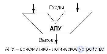
Fig.15.2. Graphic designation of the simplest ALU
4. It follows from the above that in the general case the concepts of micro-operations and microprograms are relative and require specification of the level of consideration of the processor, since a single cycle of the upper level may include several cycles of the lower level.
5. To eliminate confusion when studying the basic principles of constructing elementary processors, we will consider:
- the processor has one level;
- the processor uses one clock sequence;
- the ALU icon (see fig. 15.2) denotes a complex of combinational circuits capable of performing binary summation, a shift of the binary number, the simplest bitwise logical operations;
- microprocessor nodes that are not directly related to the control circuit, we will consider auxiliary nodes of the ALU, or, more precisely, nodes that ensure the normal functioning of the ALU.
It is obvious that various arithmetic operations on numbers (represented, besides, in a different encoding) require essentially different sequences of micro-operations. In addition, it is obvious that the more versatile an electronic device, the more complex its structure (more elements) and the slower it works. On the other hand, the functions of such a complex device can perform a set of simpler and faster devices, but the hardware costs and price will be higher.
In general, the operations performed in the ALU can be divided into the following groups:
- binary arithmetic operations for fixed-point numbers
(CHF);
- operations of binary (hexadecimal) arithmetic for numbers with
floating point (CHP);
- operations of decimal arithmetic;
- logical operations;
- operations of index arithmetic (when modifying the addresses of commands);
- special arithmetic operations: normalization of numbers,
arithmetic shift (only digits without
sign), a logical shift (all digits are shifted), etc.
General-purpose computers usually implement the operations of the above groups, but do it in different ways, depending on the type of ALU used in the processor.
ALU is divided into block and multifunctional.
In block ALUs (Fig. 15.3), the listed groups of operations are performed in separate electronic blocks, and the speed of work increases, since the blocks can perform corresponding operations in parallel. In addition, a dedicated unit always performs operations faster than a universal reconfigurable unit.
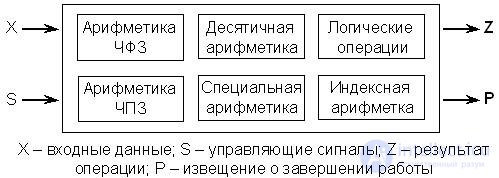
Fig.15.3. Block ALU
Block ALUs are typical for large computers, where the main thing is maximum speed, not hardware costs and costs. The simplest co-processors in a microcomputer that perform operations with a CIP can also be considered as specialized units, therefore, an ALU microcomputer with co-processors can sometimes be considered as block ones.
In the multifunctional ALU, the listed groups of operations are performed by the same circuits, which are switched as necessary depending on the required mode of operation. Such ALUs are typical for mini- and microcomputers built on simple processors.
There are other ALU structures (mixed) that are somewhere between block and multi-functional ones.
It should be borne in mind that often computers built on the basis of the simplest microprocessors have an ALU that allows them to perform only binary arithmetic operations on the PPS and some logical operations. In this case, the remaining groups of operations are performed by special subprograms, which greatly reduces the speed of their execution.
Let us consider in more detail the structure of the ALU of the simplest processor and determine the minimum necessary set of devices included in it. From the above it follows that the composition of such an ALU must include a device that performs the operations of binary summation (adder). In addition, it is necessary to have at least three buffer registers (holding registers) to store the operands and the result. However, in the simplest case, the result of the operation can be written to one of the temporary storage registers in place of one of the operands. This register is called the battery , and the processor as a whole - the processor of the battery type . The battery must necessarily have a bi-directional connection to the processor's internal data bus. (In more complex ALUs, the result of the operation can be recorded at the request of the programmer in any of the register specially allocated for this purpose). To perform arithmetic logic operations, you need a device that performs binary number shifts (shifter). And, finally, a register is needed in which some of the signs of the result of the operation performed that are necessary for the functioning of the CU (register of signs) are stored.
The block diagram of the ALU of the simplest battery-type microprocessor is shown in fig. 15.4.
It has already been noted that the ALU as a whole and the binary adder have the same designation. In accordance with the previously made observations, the temporary storage register and the battery can be considered auxiliary nodes of the ALU.
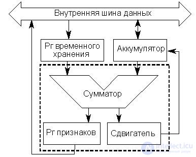
Fig.15.4. Block diagram of the simplest ALU battery type
It was noted above that the SU (Fig. 15.5) controls the work of the ALU by developing a sequence of micro-instructions necessary to perform a particular operation (+, -, /, *, etc.). The order of execution of microinstructions is determined by the firmware implementation of the operation, but may vary depending on the signs of the operation generated in the ALU (P 1 , ..., P m ) and fed to the input of the SU.
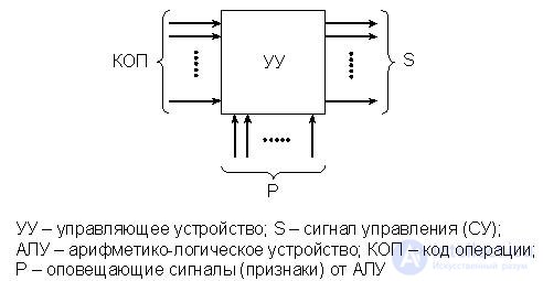
Fig.15.5. General view of the SU
Firmware can have both a linear structure and be branched, and conditional transitions are carried out in accordance with signs P.
Technical implementation of the VU, even the simplest processors are diverse. However, in the most general case, they are distinguished by the way the firmware is stored. According to this criterion, CUs are subdivided into CUs with rigid (circuit) logic and CUs with microprogram stored in special memory. If the microprocessor memory is available to the programmer, then the CUs are microprogrammable and allow changing the instruction set of the processor. If the firmware memory is not available, then the processor has an invariable system of commands, as in the case of hard logic logic controls.
These options differ from each other in construction principles, hardware costs, firmware implementation time, the ability to change the sequence of micro-instructions, and hence the processor instruction set.
UU modern processors in many cases combined. The execution of simple commands is controlled by a fast-acting CU on hard logic, and the execution of complex commands by a slower CU with firmware memory.
Below we will consider the general principles for constructing both types of CUs.
UU, built on rigid logic (Fig. 15.6), historically appeared first.
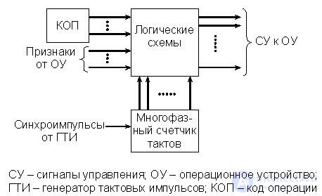
Fig.15.6. Structure of CU with rigid logic
The main advantage of such CU is their speed. That is why the absolute majority of specialized processors, especially those intended for processing information in real time, have a VU on rigid logic. Specialized processors are meant for performing a narrow set of special functions (signal processing of radar stations, Fourier transform, matrix operations, signal processing in high-speed communication lines, etc.) with maximum speed.
However, in general-purpose processors with universal instruction sets, CUs on rigid logic are also used very widely, especially, as already noted, to control the execution of simple instructions. The command systems of such processors are always fixed and cannot be changed by the user. Such SUs are sometimes called specialized.
Specialized CUs form constant control signal (SU) sequences.
The block of logic circuits consists of combinational circuits, registers, counters, decoders and other devices that perform the functions of storing the current state of the automaton determining the SU, and generating the next state in accordance with the input features.
The firmware in this machine is stored at the expense of a system of hard links between the CU nodes. To change the firmware requires the removal of hard links and the creation of a new scheme.
One of the drawbacks of VU on rigid logic is that any changes or modifications of the universal processor commands that require changes to the microprograms will lead to a change in the structure of the control automaton and, consequently, the topology of its internal connections. In the production of specialized processors, a very wide range of CUs is required (in terms of the number of problems to be solved) with a relatively small need for each specific type. From the point of view of the microelectronic production technology of processors in the form of LSIs and VLSIs, this disadvantage is very significant. The price of each released processor chip increases due to increased costs for developing new CU topologies and debugging their production technology.
The optimal solution to this problem was the construction of a CU on programmable logic structures with a fixed topology - PLA and FPGA.
The idea of creating a firmware UU arose long ago, in 1951, but was fully realized relatively recently - with the advent of compact memory devices on the LSI. A generalized block diagram of firmware CU is shown in Fig. 15.7.
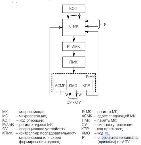
Fig.15.7. Firmware CU
In general, the MK can specify one or several MOs. The firmware is stored in the PMK. The address of the MC is formed by the KPMK controller and is stored in the address register of the MC (RgAMK). MK is read from memory in the micro-command register (RgMK). MK, in general, has three fields - ASMK, KMO, KPR.
Lastly, a sign of branching is inserted in the microprogram, which needs to be analyzed at KPMK. The address of the first MC determines the CPC, i.e. The corresponding micro subprogram is called.AFMK can be specified in MK explicitly or be formed in a natural way (with a sequential selection of MK). After issuing the control system to the control unit, the MC is executed, after which the cycle (sampling-realization) is repeated.
There are three options for the mutual arrangement of the sample-implementation cycles.
Sequential method (Fig. 15.8, a).
In this case, the sample of the next MC i + 1 is not initiated until the end of the previous MC i . The advantage of the method is primarily the simplicity of the organization of the MK-cycle.
Parallel way (MK conveyor) –pot. 15.8, b.
Имеет место совмещение этапов выборки МК i+1 и реализации МК i . При равенстве периодов выборки и реализации достигается сокращение МК-цикла теоретически в 2 раза.
Параллельно-последовательный способ (рис. 15.8, в).
Используется при наличии МК условной передачи управления, когда адрес следующей МК зависит от результата предыдущей МК. Выборка МК i+2 , стоящей после МК i+1 условного перехода, возможна только после завершения МК i+1 .
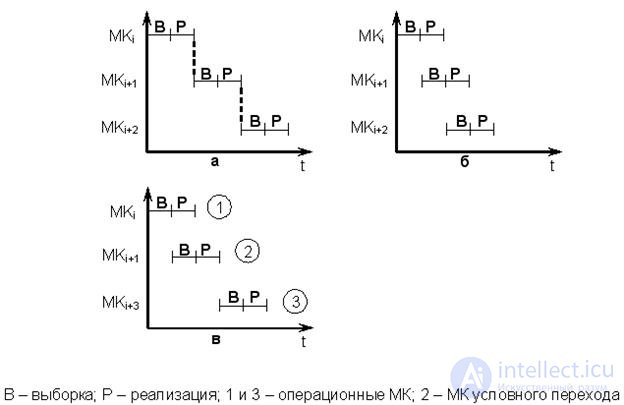
Рис.15.8. Выборка и реализация микрокоманды: а) последовательная,
б) параллельная, в) последовательно-параллельная
Используются два основных способа адресации – принудительная и естественная.
Принудительная адресация сводится к тому, что в каждой микрокоманде, включая операционные, указывается адрес следующей за ней микрокоманды (рис. 15.9, а).
Естественная адресация характерна тем, что адрес следующей микрокоманды образуется путем увеличения адреса предыдущей микрокоманды на 1. Это позволяет исключить поле адреса из операционных микрокоманд и уменьшить разрядность ПМК.
Для выполнения условных и безусловных переходов в микропрограмме используются управляющие микрокоманды, содержащие адрес перехода и поле признаков (КПР) при обоих типах адресации. Таким образом, операционные и управляющие микрокоманды должны различаться некоторым признаком (рис. 15.9, б и в). Признак a определяет тип МК (например, a = 1 – операционная).
Коротко остановимся на формировании адреса при естественной адресации. В КПМК есть специальный счетчик адреса микрокоманд (СчА), в котором в конечном итоге формируется адрес следующей микрокоманды. Алгоритм формирования адреса следующей МК зависит от ее типа, а именно:
- операционная МК – после выборки МК СчА := СчА + 1;
- управляющая МК – после выборки происходит проверка условия, заложенного в МК. Если условие выполняется, то СчА := АСМК, а если условие не выполняется, то СчА := СчА + 1.
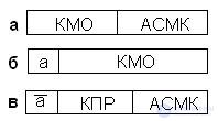
Рис.15.9. Форматы микрокоманд:
а) операционная МК при принудительной адресации;
б) операционная МК при естественной адресации;
в) управляющая МК при обоих типах адресации.
Выбор способа кодирования микрокоманд представляет собой достаточно сложную задачу и зависит от структуры процессора и его целевого назначения, системы команд, быстродействия и т.д. Рассмотрим только основные способы кодирования микрокоманд.
1. Горизонтальное кодирование (рис. 15.10, а). Это простейший вариант кодирования микрокоманд, при котором каждый разряд поля кода микроопераций однозначно определяет управляющий сигнал для выполнения микрооперации.
Достоинство данного способа состоит в том, что он допускает работу нескольких устройств, т.е. параллельное выполнение ряда МО, что повышает быстродействие.
Недостаток способа – при большом наборе МО (от нескольких десятков до нескольких сотен) возрастает разрядность МК и, следовательно, разрядность ПМК.
2. Вертикальное кодирование (рис. 15.10, б). Это другой подход к кодированию МК с целью максимального сокращения разрядности поля КМО. В этом случае требуется дешифратор МО, который увеличивает временные задержки и, следовательно, время выполнения МО.
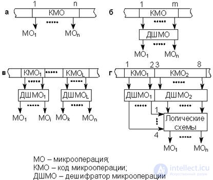
Рис.15.10. Кодирование МК: а) горизонтальное, б) вертикальное,
в) смешанное, г) косвенное
Помимо увеличения времени на МО к недостаткам следует отнести невозможность параллельного выполнения МО.
3. Смешанное кодирование (рис. 15.10, в). Это кодирование устраняет основные недостатки, присущие горизонтальному и вертикальному кодированиям.
При таком кодировании в отдельных полях кода МО объединяют взаимоисключающие наборы для обеспечения параллельного выполнения МО с разных полей. Данный способ кодирования находит широкое применение в микропрограммных УУ.
Способы 1, 2, 3 – это прямые способы кодирования. Здесь каждое поле КМО формирует определенный набор управляющих сигналов, интерпретируемых всегда одинаковым образом.
4. Косвенное кодирование (рис. 15.10, г). Этот способ кодирования позволяет еще больше уменьшить разрядность МК. Здесь одно и то же поле можно использовать для формирования СУ для различных блоков, при этом его функции определяются другим полем.
In fig. 15.10 КМО 1 кодирует одну из четырех групп МО, поле КМО 2 определяет реализуемую в данной группе операцию.
Example
 00 – микрооперации в АЛУ;
01 – МО в памяти и регистрах контроллеров периферийных устройств;
10 – МО безусловного и условного переходов;
11 – константы для загрузки регистров и счетчиков.
КМО 2 позволяет выполнить 64 МО в любой из указанных групп оборудования.
Недостатком такого способа кодирования является увеличение объема оборудования и, следовательно, дополнительных задержек при исполнении МО.
Рассмотренные способы кодирования являются одноуровневыми. На практике используют и многоуровневое кодирование (микрокоманды, нанокоманды и т. д.).
С этой точки зрения МК делятся на однофазные и многофазные. При этом в МК может быть включен дополнительный разряд, определяющий тип синхронизации.
Достоинством однофазных МК (рис. 15.11, а) является простота технической реализации.

Рис.15.11. Синхронизация МК: а) однофазная, б) многофазная
Многофазные МК (рис. 15.11, б) позволяют минимизировать число МК в памяти, упрощают выполнение сложных МК и связь между приемником и источником информации. Недостатком является увеличение объема оборудования для формирования многофазных синхросигналов.
Время выполнения некоторых МО бывает существенно меньше рабочего такта процессора (время выполнения одной МК), что позволяет при горизонтальном кодировании в одном такте выполнять не только совместимые, но и ряд несовместимых МО. Для этого рабочий такт процессора делят на подтакты (фазы), в каждом из которых выполняется одно или несколько элементарных действий (МО) по реализации МК.
1. Обобщённая структура процессора.
2. Опишите функции микропрограммного и операционного автоматов.
3. Операции, выполняемые в АЛУ.
4. Структурная схема простейшего АЛУ аккумуляторного типа.
5. Структура УУ с жёсткой логикой.
6. Микропрограммное УУ.
7. Опишите варианты взаимного расположения циклов выборка-реализация микрокоманд.
8. Два основных способа адресации микрокоманд.
9. Форматы микрокоманд при разных способах адресации.
10. Основные способы кодирования микрокоманд.
11. Варианты синхронизации выполнения микрокоманд.

Comments
To leave a comment
Computer circuitry and computer architecture
Terms: Computer circuitry and computer architecture