Lecture
In electronic computers (computers), all information is presented in a language containing only two characters of the alphabet - 0 and 1. Elements that perform the simplest operations on such characters are called logical. On the basis of logical elements computer nodes are built, designed to perform the whole variety of more complex operations performed by computers.
The theoretical basis for the construction of computer nodes is the algebra of logic developed by the English mathematician George Boole and usually called Boolean algebra . To implement a function in the form of a computer node, a logical equation is developed for this function on the basis of the laws of Boolean algebra, according to which logical elements are selected and connected.
Boolean algebra consists of the following elements:
1. numbers
2. variables
3. operations
4. expressions
5. functions
6. laws.
Consider each of the presented elements:
1. Numbers - two numbers: a logical zero (log. "0") and a logical unit (log. "1") in Boolean algebra are identified with the concepts of "true" and "false";
2. Variables - Boolean (logical, binary) variables are called variables that take values from the set zero and one {0; 1};
3. Operations - the simplest logical functions of Boolean algebra, which include:
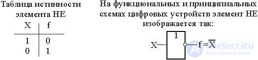
3.1. Negation (inversion):
Only the operation of negation is unary (operation with one variable). For example: operation  means negating the variable
  i.e.
i.e. 
 and vice versa - with
 . Negation can be applied to the expression -
  because expression
  can be represented as a function
  , then the inverse of the function
  will have the following form
  .
.
The operation of negation ( NOT ) f = read as f is (equivalent) NOT . The element that implements the NOT function is called the NOT element ( inverter ).
3.2. Conjunction (logical multiplication):
Conjunction and disjunction operations are performed on at least two variables or one variable and a constant.
To write a conjunction, use the following characters (sign operations):  , as well as when writing an arithmetic multiplication, lowering the multiplication operation symbol is allowed. For example, records:
  ,
,  ,
,  and
and  mean a conjunction operation on variables
  and
and  .
.
The conjunction operation ( logical multiplication) is written in the form f = X 1 · X 2 . The conjunction function is read as follows: f is (equivalent) X 1 and X 2 , since the function is true when the 1st and 2nd arguments (variables) are true. A conjunction is called an AND function, and an element that implements this function is an AND element.
In the general case, the logical multiplication function of n variables is written as:


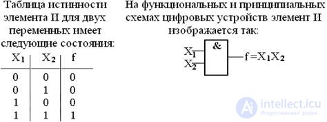
The number of variables (arguments) participating in one conjunction corresponds to the number of inputs of the And element.
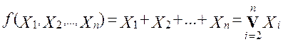
3.3. Disjunction (logical addition):
The following characters are used to write the disjunction operation:  . For example, records:
  and
and  mean the operation of disjunction over variables and .
Disjunction ( logical addition) is written as
f = X 1 + X 2 , and reads like this: f is X 1 or X 2 , because the function is true when one or another variable (at least one) is true. Therefore, the disjunction function is often called the OR function.
In the general case, the logical addition function of n variables is written as:

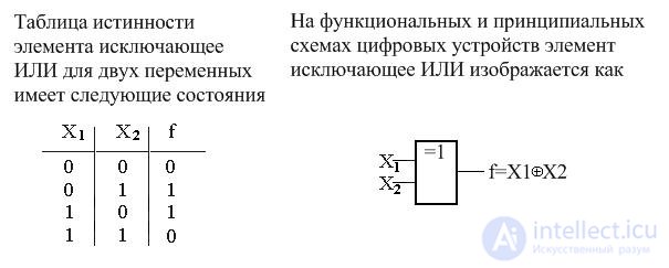
3.4. Exclusive OR (addition modulo 2)
To write an exclusive operation OR use the sign  .
.
The operation of the exclusive OR is written as f = X1  X2, and is read as f is exclusive OR from X1 and X2 , or f is equal to the sum modulo 2 X1 and X2 .
4. Expressions - variables and signed operations, joined together with the possible presence of brackets to specify the order of operations. The priority is given by the order of operation. The conjunction operation has a higher order than the disjunction operation.
5. Functions - A Boolean (logical) function is a function whose arguments are Boolean variables, and the function itself takes a value from the set {0; 1}.
The scope of the Boolean function is a collection of 2 m binary sets of its arguments. A set of arguments can be considered as an m-component binary vector.
5.1 Analytical (in the form of a logical expression) is represented as follows:  .
.
5.2 Tabular (as a truth table) representing a collection of all sets of variables and the corresponding values of a function.
The truth table contains K = 2 m rows, m columns (by the number of inputs) and one column for recording the function value.
For example: suppose you want to set the function of three variables F (X 3 , X 2 , X 1 ) (Fig. 2.1), it is implemented by a logic circuit having three inputs and one output (m = 3, K = 8).
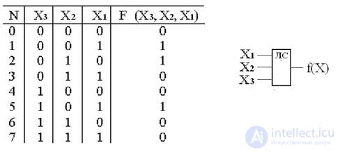
Fig.2.1. Truth table and functional designation of a logic circuit (LAN) with three inputs and one output
5.3 Numeric:
In this case, the function is specified in the form of decimal equivalents of the numbers of the sets of arguments at which the function takes a single value. For example, for the above example, the function F takes single values on sets of variables with the following numbers: 1, 2, 5, then the numerical method of the task will be : F (X 1 , X 2 , X 3 ) = (1,2,5 ) X 3, X 2, X 1 .
5.4 Graphic:
Such an approach is limited and, as a rule, is illustrative for Boolean functions of 2 and 3 variables. For example, let us present a graphical interpretation (see Fig. 2.2) of a Boolean function of 3 variables, presented in numerical form: F (x) = V (1,2,3,6,7) .
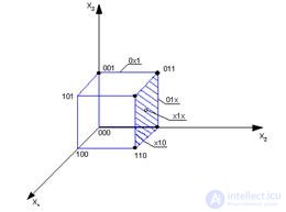
Fig. 2.2. Graphical representation of the function of three variables
5.5 Tabular graphic or coordinate:
In this method, the Boolean function is specified using a state map, which is known as a Karnaugh map or a Veitch diagram .
The Carnot map contains 2 m cells by the number of sets of variable values. Each cell is determined by the coordinates of the rows and columns corresponding to a specific set of variables. All input variables are divided into 2 groups so that one group defines the coordinates of the rows, and the other defines the coordinates of the columns. Each cell of the Carnot map is stamped with the corresponding function value on the given set. An example of setting the function of three variables is shown in Fig. 2.3. The numerical expression of this function is as follows : F (X) = (2, 3, 6) X 3, X 2, X 1 ; K = 2 m ; m = 3; K = 8.
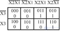
Fig. 2.3. Carnot map for the function of three variables
6. Laws (identities) of Boolean algebra:
Below are the main, most frequently used in the synthesis of combinational circuits, laws.
Transposition law:  and
and  .
.
Associative law:  and
and  .
.
Distributive law:  and
and  .
.
The law of double negation :  =
=  .
.
Tautology :  and
and  .
.
The law of the zero element :  and
and  .
.
The law of a single element :  and
and  .
.
The law of an additional element : in Boolean algebra an additional element to is an  , so:
, so:  and
and  .
.
The law of duality ( duality, de Morgan ):  and
and  .
.
As a consequence, this law implies:  and
and  .
.
The law of absorption :  and
and  .
.
Law of abbreviation :  and
and  .
.
As a consequence, this law implies:  and
and  .
.
Gluing Law:  and
and  .
.
Even the most complex transformations of digital information ultimately boil down to the simplest operations on logical variables 0 and 1. Such operations are implemented by logical elements in accordance with the formulas of the algebra of logic.
In real conditions, logical variables 0 and 1 correspond, as a rule, to different voltage levels: U 0 and U 1 . The transition from logical variables to electrical parameters raises the question of logical conventions . It is necessary to agree which of the two voltage levels should be taken as U 0 and which one as U 1 . There are agreements of positive ( positive ) and negative ( negative ) logic. It is considered that in the positive logic U 1 > U 0 , and in the negative U 1 <U 0 . It is necessary to understand that, depending on the accepted logical agreement, the same logical element performs various logical operations. Transition from operation in positive logic to operation in negative is made by inverting all variables.
In the future, if it is not specifically stated, we will use the agreements of positive logic.
The same transformations of logical variables can be defined in various forms (bases): using AND , OR , NOT operations ( Boolean basis), AND-NOT operations ( Scheffer basis), OR-NOT operations ( Pierce basis), and also many in other ways. The choice of the basis depends on the ease of implementation of a logical function using the electrical circuits of this circuit design. The most common bases are Scheffer and Pierce. In the various series of standard ICs, along with the basic logic elements, there are usually a number of others that perform other logical operations.
For proper design and operation of digital devices (DD), it is necessary to know the system of parameters of logical elements (static and dynamic).
The most important static parameters are four voltage values and four current values:
ü stress parameters:
Ø input voltage log. "1" - U in 1 ,
Ø input voltage log. “0” - U in. 0 ,
Ø output voltage log. "1" - U out.1 ,
Ø input voltage log. "0" - U vy.0 .
For normal operation of the element, it is required that the voltage corresponding to the log. "1" was quite high, and the voltage log. “0” is low enough. These requirements are set by the parameters U in. 1 min and U in. 0 max . The input voltage of this element is the output voltage of the previous (signal source). The levels guaranteed at the output of the element when the permissible load conditions are observed are set by the parameters Uout.1 min and Uout.0 max . As a rule, the output levels are somewhat “better” input, which provides a certain noise immunity of the element. For U 1, negative interference is dangerous, reducing it, and the level of permissible static interference (i.e. interference of any duration) should be. not higher than U - pom = U out. 1 min - U in. 1 min . For the level U 0, the positive are dangerous, the level of permissible static noise of which, d. no higher than U + pom = U out. 0 max - U in. 0 max .
ü current parameters:
Ø input current log. "1" - I in1 ,
Ø input current log. "0" - I in. 0 ,
Ø output current log. "1" - I out.1 ,
Ø output current log. "0" - I vy.0 .
With a high level of output voltage from the source element, the current flows out, the load circuit absorbs this current. When the output voltage of the source element is low, the load current flows into this element from the input circuits of the receiver element. Knowing the currents I out.0 max and I out.1 max , characterizing the capabilities of the source element and the currents I in. 0 max and I in. 1 max , consumed by the receiver elements, it is possible to control the observance of the load limits, mandatory for all elements of the control center .
Speed refers to the most important dynamic parameters of logical elements (LE). The speed is determined by the speed of their transition from one state to another. The speed of the CO is determined by the signal delays, as in
 LE and in the circuits of their interconnects.
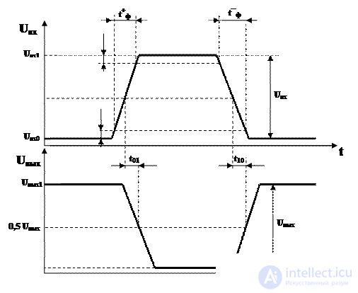
Fig. 2.4. Timing diagrams of the process of switching PE
The timing diagrams of the switching of an inverting LE (Fig. 2.4) show the durations of the characteristic stages of the transient processes, measured by the so-called measuring levels. The moment of change of a logical signal is considered the moment of reaching one of the logical levels. Often the midpoint of a threshold signal is taken as the threshold level, i.e. 0.5 (U 0 + U 1 ). Sometimes the threshold level is indicated more accurately in the passport data of the item. The time diagrams show the propagation delays when the output voltage of the element varies from U 1 to U 0 and back (t 10 + t 01 ). Very often, to simplify the calculations, the averaged value of the signal propagation delay t C = 0.5 (t 10 + t 01 ) is used.
When developing a digital device (DD), it is required to estimate its power consumption in order to formulate requirements for power sources and heat sink design. This summarizes the power dissipated by logical and other elements of the scheme. The power consumed by PE is divided into static and dynamic. Static power is consumed by PE, which does not switch. When switching, additional dynamic power is consumed, which is proportional to the switching frequency. Thus, the total power depends on the switching frequency, which should be considered when counting it.
Digital elements (logical, storage, buffer) can have outputs of the following types: logical , with the third state , with an open collector (drain) and with an open emitter (source). The presence of four types of outputs is explained by the operating conditions of the elements in logical circuits, in trunk-modular microprocessor systems, etc.
The logic output generates two levels of output voltage (U 0 and U 1 ).The output impedance of the logic output is sought to be made small, capable of developing large currents for recharging capacitive loads and, consequently, obtaining a high performance element. Most of the LEs used in combination circuits have this type of output.
The logic outputs of the TTL (W) and CMOS logic elements are similar to push-pull cascades - in them both the output voltage fronts are formed with the participation of active transistors operating in antiphase, which ensures low output resistances at any output switching voltage (see Fig. 2.5).
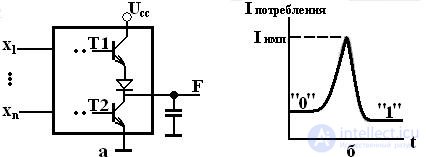
Fig. 2.5. Diagram of the output circuit of the TTL element (a) and the graph of the change in the current consumed by it in the switching process (b)
Особенность таких выходов состоит в том, что их нельзя соединить параллельно. Во-первых, это создает логическую неопределенность, т.к. в точке соединения выхода, формирующего лог. «1», и выхода, формирующего лог. «0», возникло бы их «противоборство». Во-вторых, вследствие малых величин выходных сопротивлений уравнительный ток в этом случае может достигать достаточно большой величины, что может привести к выходу из строя электрических элементов выходной цепи и, соответственно, элемента в целом.
Вторая особенность логического выхода двухтактного типа связана с протеканием через оба транзистора коротких импульсов тока при переключениях из одного состояния в другое. Эти токи протекают от источника питания на общую точку («землю»). В статических состояниях таких токов быть не может, т.к. транзисторы Т1 и Т2 работают в противофазе, т.е. один из них находится в запертом состоянии. Однако, в переходном процессе из-за некоторой несинхронности переключения транзисторов возникает кратковременная ситуация, при которой оба транзистора открыты, что и порождает короткий импульс сквозного тока, протекающего через оба транзистора, значительной величины (рис. 2.5, б).
Элементы с тремя состояниями выхода (типа ТС) кроме логического состояния «0» и «1» имеют третье состояние – «отключено» или состояние высокого импеданса (“impedance” - сопротивление), в котором ток выходной цепи пренебрежительно мал. В третье состояние элемент переводится специальным управляющим сигналом, который обеспечивает запертое состояние обоих транзисторов (Т1 и Т2 на рис. 2.5, а) Сигнал управления элементом типа ТС обычно обозначают ОЕ (Output Enable). При наличии разрешения (ОЕ=1) элемент работает в режиме логического выхода, а при его отсутствии (ОЕ=0) переходит в состояние «отключено». В ЦУ широко используются буферные элементы типа ТС для управляемой передачи сигналов по одним и тем же линиям. Буферы могут быть не инвертирующие и инвертирующие, а сигналы ОЕ H – активные (лог. «1» - высокий уровень) и L – активные (лог. «0» - низкий уровень).
Выходы типа ТС отмечаются в обозначениях элементов значком  . Их можно соединять параллельно при условии, что в любой момент времени активным может быть только один из параллельно соединенных выходов. В этом случае отключенные выходы не мешают активному формировать сигналы в точке соединения выходов, т.к. их выходное сопротивление достаточно велико.
Элементы с третьим состоянием сохраняют такие достоинства элементов с логическим выходом, как быстродействие и высокая нагрузочная способность. Поэтому они являются основными в указанных применениях. В то же время они требуют обязательного соблюдения условия отключения всех выходов, соединенных параллельно, кроме одного, т.е. условия ОЕ 1 + ОЕ 2 +…+ ОЕ n ≤1 при объединении n выходов. Нарушение этого условия может привести даже к выходу из строя элементов.
Элементы с открытым коллектором имеют выходную цепь, заканчивающуюся одиночным транзистором, коллектор которого не соединен с какими-либо цепями внутри микросхемы (рис. 2.6,а).
Транзистор управляется от предыдущей части схемы элемента так, что может находиться в насыщенном или запертом состоянии. Насыщенное состояние транзистора соответствует лог. «0», а запертое – лог. «1». Насыщение транзистора обеспечивает на выходе малый уровень напряжения (напряжение насыщения «коллектор – эмиттер»). Запирание же транзистора какого-либо напряжения на выходе не задает, выход при этом имеет фактически неизвестный «плавающий» потенциал, т.к. не подключен к каким-либо цепям схемы элемента. Поэтому для формирования высокого уровня напряжения при запирании транзистора на выходе элементов с открытым коллектором (типа ОК) требуется подключать внешние резисторы (или другие нагрузки), соединенные с источником питания.

Fig. 2.6. Схема выходной цепи элемента с открытым коллектором (а) и реализация монтажной логики (б)
Несколько выходов типа ОК можно соединить параллельно, подключая их к общей для всех выходов цепочке U cc -R (рис. 2.6,б). При этом можно получить режим поочередной работы элементов на общую линию, как для элементов типа ТС, если активным будет лишь один элемент, а выходы всех остальных окажутся запертыми. Если же разрешить активную работу всем элементам, подключенным к одной линии, то можно получить дополнительную логическую операцию, так называемую операцию монтажной логики .
При реализации монтажной логики высокое напряжение на общем выходе возникает только в том случае, когда заперты выходные транзисторы всех элементов, электрически соединенных по выходу, т.к. насыщение хотя бы одного из них снижает выходное напряжение до уровня U 0 = U кэн . Those. для получения лог. «1» на выходе требуется состояние лог. «1» на всех выходах. Таким образом выполняется монтажная операция И. Поскольку каждый элемент выполняет операцию Шеффера (И-НЕ) над своими входными переменными, общий результат будет следующим:

В обозначении элементов с ОК после символа функции ставится ромб с черточкой снизу. In fig. 2.6,б изображены элементы монтажной логики И-НЕ.
При использовании элементов с ОК в магистрально-модульных структурах требуется разрешать или запрещать работу того или иного элемента. Для элементов типа ТС это делалось с помощью специального сигнала ОЕ. Для элементов типа ОК в качестве входа ОЕ может быть использован один из обычных входов элемента. Если речь идет об элементе И-НЕ, то, подавая лог. «0» на любой из входов, можно запретить работу элемента, поставив его выход в разомкнутое состояние независимо от состояния других входов. Лог. «1» на этом входе разрешит работу элемента.
Положительными свойствами элементов с ОК при работе в магистрально-модульных системах является их защищенность от повреждений из-за ошибок управления, приводящих к одновременному подключению к магистрали нескольких элементов, а также возможность реализации дополнительных операций монтажной логики. Недостатком таких элементов является большая задержка переключения из лог. «0» в лог. «1». При этом переключении происходит заряд выходной емкости сравнительно малым током, протекающим через резистор R, сопротивление которого нельзя сделать слишком малым, т.к. это приведет к большим токам выходной цепи в статике при насыщенном состоянии выходного транзистора. Значение сопротивления резистора R проектировщик при работе с элементами типа ОК выбирает с учетом требуемого быстродействия схемы и потребляемой ею мощности. При этом, выбор значения сопротивления, близкого к минимально допустимому позволит достичь максимального быстродействия, а к максимально допустимому – к минимальной мощности потребления.
Выход с открытым эмиттером характерен для элементов типа ЭСЛ
( эмиттерно-связанная логика). Для работы на магистраль такие элементы не используются. Возможность соединять друг с другом выходы с открытым эмиттером при объединении эмиттерных резисторов в один общий резистор приводит к схеме, используемой при построении логических схем для получения дополнительной операции монтажной логики (рис. 2.7).
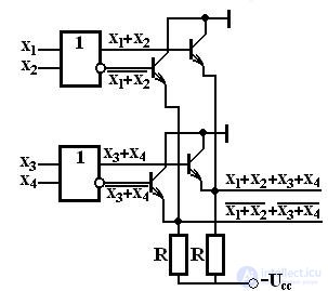
Fig. 2.7. Схема выходного цепи элемента с открытым эмиттером
Элементы ЭСЛ имеют противофазные выходы, на одном из которых реализуется функция ИЛИ, на другом – ИЛИ-НЕ. Соединяя прямые выходы нескольких элементов, получают расширение по ИЛИ (входные элементы нескольких элементов образуют единую дизъюнкцию). Соединяя инверсные выходы, получают операцию И-ИЛИ относительно инверсных входных переменных т.к. при этом:
 .
.
Соединяя прямой выход одного элемента с инверсным выходом второго элемента, можно получить функцию вида:
 .
.
При построении КС устройств вычислительной техники используются различные логические элементы, которые должны согласоваться по входным и выходным сигналам, напряжению питания и т.д. Для этой цели логические элементы объединяют в серии.
Серией (системой, комплексом) логических элементов ЭВМ называется предназначенный для построения цифровых устройств функционально полный набор логических элементов, объединяемый общими электрическими, конструктивными и технологическими параметрами, использующий одинаковый способ представления информации, одинаковый тип межэлементных связей. Система элементов чаще всего избыточна по своему функциональному составу, что позволяет строить схемы более экономичные по количеству использованных элементов.
В состав серии входят элементы для выполнения логических операций, запоминающие элементы, элементы, реализующие функции узлов ЭВМ, а также специальные элементы для усиления, восстановления и формирования сигналов стандартной формы.
Конструктивно логические элементы представляют собой микроминиатюризированые интегральные электронные схемы (микросхемы), сформированные в кристалле кремния с помощью специальных технологических процессов.
В большинстве современных серий элементов имеются микросхемы малой степени интеграции (ИС до 100 элементов на кристалле), средней степени (СИС – до 1000 элементов на кристалле), большой степени интеграции (БИС – до 10000 элементов на кристалле) и сверхбольшой степени интеграции (СБИС – более 10000 элементов на кристалле). Логические элементы в виде ИС реализуют совокупность простых логических операций: И, ИЛИ, И-ИЛИ, И-НЕ, ИЛИ-НЕ и т.д. Логические элементы на СИС и БИС реализуют узлы ЭВМ, на СБИС – микроЭВМ.
Основными параметрами серии логических элементов являются:
Ø питающие напряжения и сигналы для представления лог. «0» и лог. «1»;
Ø коэффициенты объединения по входу;
Ø нагрузочная способность (коэффициент разветвления по выходу);
Ø помехоустойчивость;
Ø рассеиваемая мощность;
Ø быстродействие.
Серия элементов характеризуется количеством используемых питающих напряжений и их номинальными значениями. Обычно лог. «0» соответствует низкий уровень напряжения, а лог. «1» – высокий. Для наиболее часто используемых серий напряжение питания составляет +5В, уровень логической единицы 2,4-5В, уровень логического 0 – 0-0,4В.
Коэффициент объединения по входу ( К об ) определяет максимально возможное число входов логического элемента, иными словами, функцию скольких переменных может реализовать этот элемент. Обычно К об принимает значение от 2 до 4, реже К об = 8. Увеличение числа входов связано с усложнением схемы элементов и приводит к ухудшению других параметров – помехоустойчивости, быстродействия и т.д.
Коэффициент разветвления по выходу (К раз ) показывает на какое количество логических входов может быть одновременно нагружен выход данного логического элемента. Обычно К раз для наиболее часто используемых серий равен 10. Иногда вместо К раз задается предельно допустимое значение выходного тока логического элемента в состоянии «0» или «1».
Помехоустойчивость – это способность элемента правильно функционировать при наличии помех. Она определяется максимально допустимым напряжением помехи, при котором не происходит сбоя в его работе. Обычно это напряжение порядка 0,6-0,9 В.
Быстродействие логических элементов является одним из важнейших параметров и характеризуется временем задержки распространения сигнала. Этот параметр существенно зависит от технологии изготовления микросхем и лежит в диапазоне от единиц до сотен наносекунд.
Сравнительные характеристики наиболее употребляемых серий логических элементов приведены в табл.2.1., где в первой колонке приведены зарубежные обозначения серий, во второй – отечественные.
| Отечест венный аналог | Напря жение питания Vcc+_10%, B | Совместимость | Входной ток~ I IL /I IH , мкА/мкА | Нагрузка~ I OL /I OH , мА/мА | Ток потреб- ления~ I CC , мкА | Быс тро дейст вие, нс | |||||||||||||||||||||||||||||||||||||||||||||||||||||||||||||||||||||||||||||||||||||||||||||||||||||||||||||||||||||||||||||||||||||||||||||||||||||||||||||||||||||||||||||
| по входам V IL /V IH | по выходам V OL /V OH | ||||||||||||||||||||||||||||||||||||||||||||||||||||||||||||||||||||||||||||||||||||||||||||||||||||||||||||||||||||||||||||||||||||||||||||||||||||||||||||||||||||||||||||||||||
| BICMOS | |||||||||||||||||||||||||||||||||||||||||||||||||||||||||||||||||||||||||||||||||||||||||||||||||||||||||||||||||||||||||||||||||||||||||||||||||||||||||||||||||||||||||||||||||||
| ABT LVT(16) | - - | 5 3,3 | TTL TTL,CMOS | TTL TTL,CMOS | -5/5 -5/1 | 64/-32 64/-32 | 30 mA 9,0 mA | 3,6 4,1 | |||||||||||||||||||||||||||||||||||||||||||||||||||||||||||||||||||||||||||||||||||||||||||||||||||||||||||||||||||||||||||||||||||||||||||||||||||||||||||||||||||||||||||
| CMOS | |||||||||||||||||||||||||||||||||||||||||||||||||||||||||||||||||||||||||||||||||||||||||||||||||||||||||||||||||||||||||||||||||||||||||||||||||||||||||||||||||||||||||||||||||||
|
|
|
|
|
|
|
|
| |||||||||||||||||||||||||||||||||||||||||||||||||||||||||||||||||||||||||||||||||||||||||||||||||||||||||||||||||||||||||||||||||||||||||||||||||||||||||||||||||||||||||||
| Биполярные | |||||||||||||||||||||||||||||||||||||||||||||||||||||||||||||||||||||||||||||||||||||||||||||||||||||||||||||||||||||||||||||||||||||||||||||||||||||||||||||||||||||||||||||||||||
|
|
|
|
|
|
|
| ||||||||||||||||||||||||||||||||||||||||||||||||||||||||||||||||||||||||||||||||||||||||||||||||||||||||||||||||||||||||||||||||||||||||||||||||||||||||||||||||||||||||||||
1. Назовите элементы, из которых состоит Булева алгебра.
2. Give the definition of the simplest logical functions of Boolean algebra.
3. List the forms for setting Boolean functions.
4. Give a definition and give an example of a table form for setting the Boolean function.
5. What is the difference between the numerical and analytical forms of setting Boolean functions.
6. Give an example of the coordinate form of the Boolean function.
7. Write down the basic laws of Boolean algebra.
8. What is the difference between positive and negative logic?
9. What is the difference between different types of output stages of logic elements?
10. What are assembly logic operations.
11. What is called a series of logical elements.
12. List the basic parameters of a series of logical elements.
13. Give the definition of the branching ratio for the output.

Comments
To leave a comment
Computer circuitry and computer architecture
Terms: Computer circuitry and computer architecture