Lecture
Computer memory is a collection of devices that serve for storing, storing and issuing information. Separate devices included in this set are called storage devices (memories) or memories of one type or another. At present, both memory and memory have become almost synonymous.
The performance of a computer and its capabilities depend to a large extent on the characteristics of the charger, and in any general-purpose computer several types of chargers are used.
Basic operations:
- Record - entering information into memory;
- Reading - retrieving information from memory.
Both of these operations are generally referred to as memory accesses .
When accessing the memory, a certain unit of data is read or written, which is different for devices of different types. Such a unit can be a byte, a machine word, a data block.
Let us briefly review the most important characteristics of a memory device - capacity, specific capacity, speed, which are typical for any type of memory, as well as some methods for their classification.
· Memory capacity is determined by the maximum amount of data that can be stored in it simultaneously. Capacity is measured in bits, bytes, machine words (this was discussed at the very beginning of the course). Usually, larger units of measure are used: 1K = 1024 (Kb, Kb, Kslov),
1024 KB = 1 MB, 1024 MB = 1 GB.
· Specific capacity is defined as the ratio of the capacity of the charger to its physical volume and characterizes the degree of technological perfection of the charger.
· Specific cost is defined as the ratio of the cost of the charger to its capacity and determines, in addition to technological perfection, the competitiveness of the product on the market.
· Memory speed determines the duration of the access operation and is divided into:
- at the time of circulation when reading  . This is the time required to search for the desired unit of information and its reading;
- time of access during recording  . This is the time it takes to find a place to store a given unit of information and to write it into memory.
In some memory devices, reading information is accompanied by its destruction (erasure). In this case, the cycle of access to the memory when reading must contain the operation of regeneration of the read information in the same place in the memory. In some cases, the memory requires before storage to bring the storage elements in a certain initial state. In this case, the cycle of accessing the memory during recording must contain the operations of preparing the storage elements for the write operation itself.
In general, the duration of a read-access memory cycle consists of the following components:
 ,
,
Where  - access time when reading - the time interval between the start of the circulation operation when reading and the moment when access to this unit of information became possible;
 - the duration of the physical reading process itself, i.e. the process of detecting and fixing the state of the corresponding storage elements or portions of the surface of the carrier;
 - time to restore destroyed when reading information. In memory without destruction
  .
.
The duration of a memory access cycle when recording information generally consists of the following components:
 ,
,
Where  - access time when recording - the time interval from the beginning of the call to the moment when it becomes possible to access the storage element or the surface area of the medium in which recording is made;
 - the time interval required to reset the storage elements or sections of the surface of the carrier for recording this unit of information;
 - the duration of the physical recording process itself, i.e. time to change the physical state of the storage elements or the surface area of the carrier.
In most cases
 .
.
As the duration of the memory access cycle , the value is taken
 .
.
It should be borne in mind that for storage of information in a computer, memory devices are used that are built on different principles of operation and have a variety of technical and structural implementations. In addition, they are all sophisticated electronic devices. Therefore, memory devices have numerous characteristics, each of which can be used to classify devices. Below, we will consider only the main criteria by which it is customary to qualify the memory, namely: by the principle of operation, by the realization in the memory of the operations of circulation, by the method of access to the stored information.
1 . Operating principle. On this basis, the main types of memory, the most widely used in modern computers, are divided:
· Electronic, in which semiconductors are used as storage elements;
· Magnetic with fixed memory elements;
· Magnetomechanical with moving magnetic data carriers;
· Optical with a moving information carrier;
· Magneto-optical with moving information carrier.
In the absolute majority of cases electronic memory on semiconductor elements is used as an internal computer memory. In rare cases, specialized control computers use memory with fixed magnetic storage elements. The remaining types of devices are used as external computer memories.
Numerous "unconventional" chargers are being developed and explored, namely: chargers on charge-coupled devices, acoustoelectronic chargers, piezoelectronic chargers, magnetoelectronic chargers, etc.
2. The way to implement in-memory operations of circulation . On this basis are distinguished:
· Random access memory, allowing both reading and writing information (RAM). These are volatile memory devices (the information in them is stored only when power is available), which are used to build operational storage devices (RAM), cache, super-operative memory (SOP), etc.
· The memory is permanent, allowing only the reading of the information embedded in it in the process of manufacturing or setting (ROM). These are non-volatile memories (information is stored in them in the absence of power), which, in turn, are divided into permanent memory (ROM, EPROM) and reprogrammable memory (PROM, EEPROM). RAM and ROM performance is about the same.
· Flash EPROM (Flash EEPROM) - non-volatile reprogrammable memory, information in which is stored up to several years. Appeals to them are possible both for writing and reading. However, the speed of these memories is lower than that of RAM and ROM. Usually flash is used to accumulate information. The number of flash overwrites is limited.
3. The way to organize access . On this basis, memory is distinguished from direct (arbitrary), direct (cyclic) and sequential access.
· Direct (random) access. In the memory of this type, the access time, and therefore the access cycle, does not depend on the location of the memory element from which information is read or written to. In most cases, this is electronic memory, in which direct access is realized using electronic logic circuits. In a random access memory, the circulation cycle is from 1-2 µs to a few
nanoseconds
Independence  from the position of the storage element in the storage array takes place only up to a certain frequency of processor accesses to the memory. With an increase in the frequency of references to units of nanoseconds, the geometrical position of the storage element in the array begins to affect. This is primarily due to the final speed of propagation of an electrical signal in an insulated conductor, which is about 60% of the speed of light.
The number of bits read or written to a random access memory in parallel with time during a single access operation is called the sample width .
In other types of memory, slower electromechanical processes are used, therefore the circulation cycle is longer.
· Direct (cyclic) access. This type of memory includes devices on magnetic, optical and magneto-optical disks, as well as on magnetic drums (the latter are currently used very rarely). Due to the continuous rotation of the information carrier, the possibility of accessing a certain section of the medium for reading or writing is cyclically repeated. In such a memory, the access time is usually from fractions of a second to units of a millisecond.
· Serial access. This type of storage device includes magnetic tape devices. In the access process, a sequential viewing of sections of the information carrier is carried out until the required section takes up some initial position. The worst access time is minutes, as the tape recorder will have to rewind the entire tape.
The classical five-block structure of Neumann, considered earlier, assumed the presence of only one memory device - OP. However, modern computers have a hierarchical memory structure, each level of which is characterized by a different speed and capacity. The emergence of numerous hierarchically located memory levels is primarily associated with a constant increase in the gap in processor speed and RAM, which must be compensated for in order to improve the performance of the computer as a whole.
In addition, the development of software and the expansion of the range of tasks solved on a computer, demanded a constant increase in the volume of EP. Meanwhile, it is known that throughout the development of a computer, the requirements for capacity and speed of memory were contradictory - the higher the speed, the more difficult and more technically difficult and expensive the increase in capacity is. The need to maintain the cost of computer memory at an acceptable level, as well as many technical problems associated with the construction of high-speed memory of large volume, and led in the process of evolution to the creation of a hierarchical memory structure of modern computers.
Despite significant differences in the principles of functioning and technical implementation of different memory levels, there are general principles for constructing the entire hierarchy:
- the closer the memory level to the processor, the higher its speed and less capacity;
- the interaction algorithms of all memory levels are constructed so that the number of accesses of the upper, faster speed to the underlying, less fast, adjacent level is minimal;
- the exchange of information between adjacent hierarchical levels of memory in most cases is carried out in blocks of fixed length, which allows speeding up the exchange due to the hardware implementation of the algorithms.
In general, the memory of a modern computer includes the following hierarchical levels:
· Overactive memory (SOP), which is also called local memory.
· Cache memory, which is usually absent in the simplest processor devices. In more complex computers, the cache has several levels, and the top-level cache is always in the processor chip.
· Operational (main) memory (RAM) or random access memory (RAM), as well as a system ROM combined with RAM by a common address field.
· Memory with direct access on magnetic disks.
· Memory with sequential access on magnetic tapes.
Devices are listed in decreasing order of speed and volume.
Let us consider in the most general terms the functional purpose of the memory devices shown in fig. 14.1.
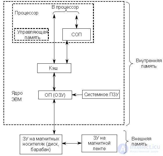
Fig.14.1 Hierarchical structure of memory
Operational (main) memory, system ROM. The name of this memory device (OP) reflects the fact that the processor can only work with programs that are loaded into the OP. This principle was the basis for the functioning of the first single-task computers. By the same principle, modern multi-tasking single-processor systems function. In the absence of the cache OP serves to store information directly used in the computing process. Operands and commands come from the OP to the processor, and vice versa - the results of the operations performed.
The characteristics of the OP directly affect the characteristics of the computer as a whole and, above all, the performance (even if there is a cache).
The amount of OP depends on the purpose of the computer and varies in a very wide range - from dozens of KB in the simplest controllers to hundreds of MB. In modern computers, the OP is always performed on semiconductor chargers and has a cycle time of no more than 1–2 μs. (In the first-generation computer, the OP was built first on electron tubes and then on ferrite rings).
System ROM has a common address space with RAM (RAM). Its volume and filling significantly depend on the purpose of the computer.
The system ROM can store the operating system kernel, utilities, drivers, utility and application programs, etc. When the computer is turned on or its operation, the programs recorded in the system ROM are in most cases loaded into the RAM (RAM) and only after that are processed by the processor.
Super-fast memory. The need for SOPs arose already in the first computers, when the speed of the processor exceeded the speed of the OP. Modern SOPs are always built on semiconductors and are sets of registers inside a processor chip in close proximity to the ALU and CU. The speed of the SOP should correspond to the speed of the ALU and the processor UU. The cycle of the appeal to the SOP is 1-2 cycles. The volume of SOP is very small. In many cases, SOP is also called the processor's internal register memory . SOP registers are used to temporarily store the results of an operation in an ALU, operands, service constants, very short instruction sets of the program being processed, etc. At its core, SOP is a buffer memory, which to some extent smoothes the gap in processor and RAM performance. However, its insignificant volume does not allow to obtain an acceptable solution to the problem, therefore, in the process of computer evolution, another hierarchical level of buffer memory emerged, whose speed is slightly lower than the SOP, and the capacity is much higher.
Cache memory This type of memory is a high-speed buffer of sufficiently large volume between the processor (its internal memory) and a relatively slow-acting RAM. Its volume (single-level cache) is about 16-256 Kbytes at 4-8 MB of OP. This memory is not available to the programmer ( cash in translation means a cache ). The cache memory, as already noted, is located in the immediate vicinity of the processor, and the upper level cache is located directly in the processor chip. Currently, top-level cache and SOP have become virtually a single hierarchical level of internal memory of the processor. In the IBM PC LSI, the lower level cache is located on the processor bus. Information in the cache memory is pumped from the OP in small blocks, while unnecessary blocks are removed from the cache back to the OP. The presence of the cache memory allows to smooth the difference in processor speed and RAM. In addition, the cache memory makes it possible in some cases not to interrupt the operation of the processor when exchanging external devices with an OP in direct access mode (DMA).
External memory . The need for memory, the volume of which would substantially exceed the size of the existing OP, arose during the operation of the first computers. Such memory could solve many problems associated with the introduction of large programs into the computer, which could not be placed in the OP, and especially with the storage of large data sets. Initially, magnetic drum (NMB) and magnetic tape (NML) drives were used as external computer memory. Then hard disk drives and flexible magnetic disks (HDDs) were developed and created, which intensively replaced the slower NMLs. Subsequently, optical and magneto-optical disk drives were created.
Currently, the main type of external memory device is NMD. External memory on NMD is sometimes called an operational external storage device (OVC). NML began to be used as archive STIs (streamers) intended for backup storage of information. The same class of OVDs include drives on optical and magneto-optical disks. All of the OVCs listed above are many times slower than the OD, and the information stored on them cannot be directly processed by the processor. Before processing in the processor information from the OVC must be necessarily placed in the OP. Емкость ВЗУ в ряде случаев для конкретной ЭВМ и конкретной задачи можно считать бесконечной.
Ниже рассматриваются принципы построения только внутренней памяти ЭВМ.
Функционально ЗУ любого типа всегда состоят из запоминающего массива, хранящего информацию, и вспомогательных, весьма сложных блоков, служащих для поиска в массиве, записи и считывания (и, если требуется, для регенерации).
Запоминающий массив (ЗМ) состоит из множества одинаковых запоминающих элементов (ЗЭ). Все ЗЭ организованы в ячейки, каждая из которых предназначена для хранения единицы информации в виде двоичного кода, число разрядов которого определяется шириной выборки. Способ организации памяти зависит от методов размещения и поиска информации в ЗМ. По этому признаку различают адресную, ассоциативную и стековую память.
В памяти с адресной организацией размещение и поиск информации в ЗМ основаны на использовании адреса хранения единицы информации, которую в дальнейшем для краткости будем называть словом . Адресом служит номер ячейки ЗМ, в которой это слово размещается. При записи (считывании) слова в ЗМ инициирующая эту операцию команда должна указывать адрес (номер) ячейки, по которому надо произвести запись (считывание).
In fig. 14.2 изображена обобщенная структура адресной памяти.
Цикл обращения к памяти инициализируется поступающим в БУП сигналом "Обращение". Общая часть цикла обращения включает в себя прием в РгА с шины адреса (ША) адреса обращения и прием в БУП управляющего сигнала "Операция", указывающего вид запрашиваемой операции (считывание или запись).
Считывание . БАВ дешифрирует адрес и посылает сигнал, выделяющий заданную адресом ячейку ЗМ. В общем случае БАВ может также посылать в выделенную ячейку памяти сигналы, настраивающие ЗЭ ячейки на запись или считывание. После этого записанное в ячейку слово считывается усилителями БУС и передается в РгИ. Затем в памяти с разрушающим считыванием происходит регенерация информации путем записи слова из РгИ через БУЗ в ту же ячейку ЗМ. Операция считывания завершается выдачей слова из РгИ на выходную информационную шину ШИ вых .
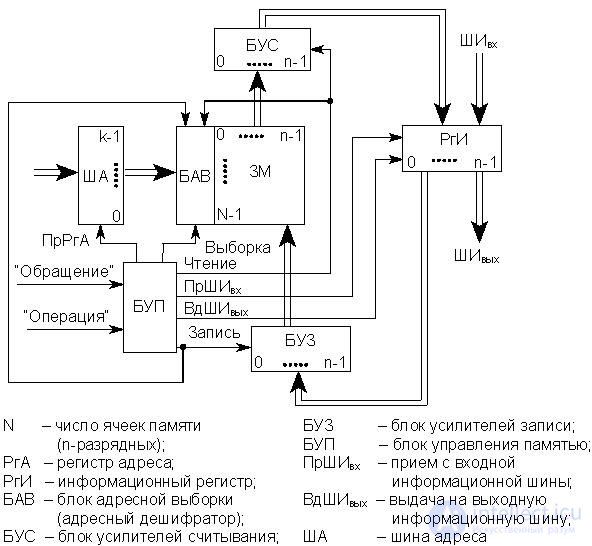
Рис.14.2. Обобщённая структура адресного ЗУ
Запись. Помимо указанной выше общей части цикла обращения происходит прием записываемого слова с входной шины ШИ вх в РгИ. Сама запись в общем случае состоит из двух операций – очистки ячейки и собственно записи. Для этого БАВ сначала производит выборку и очистку ячейки, заданной адресом в РгА. Очистка ячейки ЗМ (приведение в исходное состояние) может осуществляться по-разному. В частности, в памяти с разрушающим считыванием очистку можно производить сигналом считывания слова в ячейке при блокировке БУС (чтобы в РгИ не поступила информация). Затем в выбранную ячейку записывается новое слово.
Необходимость в операции очистки ячейки перед записью, так же как и в операции регенерации информации при считывании, определяется типом используемых ЗЭ, способами управления, особенностями электронной структуры БИС памяти, поэтому в полупроводниковых памятях эти операции могут отсутствовать.
БУП генерирует необходимые последовательности управляющих сигналов, инициирующих работу отдельных узлов памяти. Следует иметь в виду, что БУП может быть весьма сложным устройством (своеобразным управляющим контроллером, имеющим собственную кэш-память), придающим БИСу памяти в целом специальные потребительские свойства, такие как многопортовость, конвейерная выдача информации и т.п.
В памяти этого типа поиск информации происходит не по адресу, а по ее содержанию. Под содержанием информации в данном случае понимается не смысловая нагрузка лежащего на хранении в ячейке памяти слова, а содержание ЗЭ ячейки памяти, т.е. побитовый состав записанного двоичного слова. При этом ассоциативный запрос (признак) также представляет собой двоичный код с определенным побитовым составом. Поиск по ассоциативному признаку происходит параллельно во времени для всех ячеек ЗМ и представляет собой операцию сравнения содержимого разрядов регистра признака с содержимым соответствующих разрядов ячеек памяти. Для организации такого поиска все ЗЭ ЗМ снабжены однобитовыми процессорами, поэтому в ряде случаев память такого типа рассматривают как многопроцессорную систему.
Полностью ассоциативная память большого объема является очень дорогостоящим устройством, поэтому для ее удешевления уменьшают число однобитовых процессоров до одного на ячейку памяти. В этом случае сравнение ассоциативного запроса с содержимым ячеек памяти идет последовательно для отдельных разрядов, параллельно во времени для всех ячеек ЗМ.
При очень больших объемах памяти на определенных классах задач ассоциативный поиск существенно ускоряет обработку данных и уменьшает вероятность сбоя в ЭВМ. Кроме того, ассоциативные ЗУ с блоками соответствующих комбинационных схем позволяют выполнить в памяти достаточно сложные логические операции: поиск максимального или минимального числа в массиве, поиск слов, заключенных в определенные границы, сортировку массива и т.д.
Следует отметить, что ассоциативный поиск можно реализовать и в компьютере с обычной адресной памятью, последовательно вызывая записанные в ячейки памяти слова в процессор и сравнивая их с некоторым ассоциативным признаком (шаблоном). Однако при больших объемах памяти на это будет затрачено много времени. При использовании ассоциативной памяти можно, не считывая слов из ОП в процессор, за одно обращение определить количество слов, отвечающих тому или иному ассоциативному запросу. Это позволяет в больших базах данных очень оперативно реализовать запрос типа: сколько жителей области не представило декларацию о доходах и т.п.
В некоторых специализированных ЭВМ ОП или его часть строится таким образом, что позволяет реализовать как ассоциативный, так и адресный поиск информации.
A simplified structural diagram of an associative memory, in which all ZE 3M are equipped with single-bit processors, is shown in Fig. 14.3.
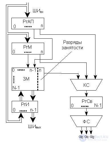
Fig.14.3. Generalized structure of associative memory
Initially, consider an operation called association control . This operation is common to the operation of reading and writing, and also has independent significance.
По входной информационной шине в РгАП поступает n-разрядный ассоциативный запрос, т.е. заполняются разряды от 0 до n-1. Одновременно в РгМ поступает код маски поиска, при этом n-й разряд РгМ устанавливается в 0. Ассоциативный поиск производится лишь для совокупности разрядов РгАП, которым соответствуют 1 в РгМ (незамаскированные разряды РгАП). Для слов, в которых цифры в разрядах совпали с незамаскированными разрядами РгАП, КС устанавливает 1 в соответствующие разряды РгСв и 0 в остальные разряды.
Комбинационная схема формирования результата ассоциативного обращения ФС формирует из слова, образовавшегося в РгСв, как минимум три сигнала:
- a 0 – отсутствие в ЗМ слов, удовлетворяющих ассоциативному признаку;
- a 1 – наличие одного такого слова;
- a 2 – наличие более чем одного слова.
Возможны и другие операции над содержимым РгСв, например подсчет количества единиц, т.е. подсчет слов в памяти, удовлетворяющих ассоциативному запросу, и т.п.
Формирование содержимого РгСв и a 0 , a 1 , a 2 по содержимому РгАП, РгМ, ЗМ и называется операцией контроля ассоциации.
Считывание. Сначала производится контроль ассоциации по признаку в РгАП.
Затем:
- a 0 = 1 – считывание отменяется из-за отсутствия искомой информации;
- a 1 = 1 – считывается в РгИ найденное слово, после чего выдается на ШИ вых ;
- a 2 = 1 – считывается слово, имеющее, например, наименьший номер среди ячеек, отмеченных 1 в РгСв, после чего выдается на ШИ вых .
Запись. Сначала отыскивается свободная ячейка (полагаем, что в разряде занятости свободной ячейки записан 0). Для этого выполняется контроль ассоциации при РгАП=111...10 и РгМ=000...01, т.е. n-й разряд РгАП устанавливается в 0, а n-й разряд РгМ – в 1. При этом свободная ячейка отмечается 1 в РгСв. Для записи выбирают свободную ячейку, например, с наименьшим номером. В нее записывается слово, поступившее с ШИ вх в РгИ.
Следует отметить, что на данной схеме не изображены блоки БУП, БУС, БУЗ, которые есть в реальных устройствах. Кроме того, для построения ассоциативной памяти требуются запоминающие элементы, допускающие считывание без разрушения.
Стековая память, так же как и ассоциативная, является безадресной. Стековая память может быть организована как аппаратно, так и на обычном массиве адресной памяти.
В случае аппаратной реализации ячейки стековой памяти образуют одномерный массив, в котором соседние ячейки связаны друг с другом разрядными цепями передачи слов (рис. 14.4). При этом возможны два типа устройств (а, б), принципы функционирования которых различны. Рассмотрим первоначально структуру на рис. 14.4, а.
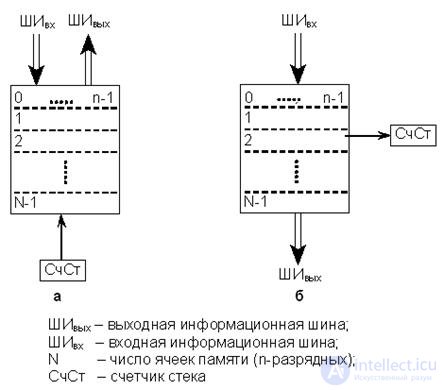
Рис.14.4. Обобщенная структура аппаратного стека: а) стек LIFO,
б) стек FIFO
Запись нового слова, поступившего с ШИ вх , производится в верхнюю (нулевую) ячейку, при этом все ранее записанные слова (включая слово в ячейке 0) сдвигаются вниз, в соседние ячейки, номера которых на единицу больше. Считывание возможно только из верхней (нулевой) ячейки памяти. Основной режим – это считывание с удалением. При этом все остальные слова в памяти сдвигаются вверх, в соседние ячейки с меньшими номерами. В такой памяти реализуется правило: последний пришел – первый ушел . Стеки подобного типа принято называть стеками LIFO (Last In – First Out).
В ряде случаев устройства стековой памяти предусматривают также операцию простого считывания слова из ячейки 0 без его удаления и сдвига остальных слов. При использовании стека для запоминания параметров инициализации контроллеров каких-либо устройств ЭВМ обычно предусматривается возможность считывания содержимого любой ячейки стека без его удаления, т.е. считывание содержимого не только ячейки 0.
О первом слове, посылаемом в стек, говорят, что оно располагается на дне стека . О последнем посланном (по времени) в стек слове говорят, что оно находится в вершине стека . Таким образом, ячейка N-1 – дно стека, а ячейка 0 – вершина.
Обычно аппаратный стек снабжается счетчиком стека СчСт, показывающим общее количество занесенных в память слов (СчСт = 0 – стек пустой). При заполнении стека полностью он запрещает дальнейшие операции записи.
Стековый принцип организации памяти можно реализовать не только в специально предназначенных для этого устройствах. Стековая организация данных возможна и на обычной адресной памяти с произвольным обращением (программный стек). Для организации стека LIFO в этом случае необходима еще одна ячейка памяти (регистр), в которой всегда хранится адрес вершины стека и которая называется указателем стека . Обычно в качестве указателя стека используют один из внутренних регистров процессора. Кроме этого, требуется соответствующее программное обеспечение. Принципы стековой организации данных на обычной адресной памяти иллюстрируются схемой на рис. 14.5.
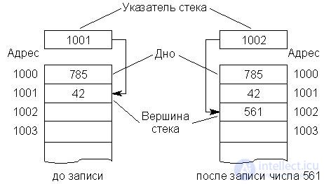
Рис.14.5. Запись слова в программный стек LIFO
Unlike the hardware stack, the data placed on the software stack does not move when a new number is written or read. Each new word is written in the memory cell, the next in order after the one whose address is contained in the stack pointer. After writing a new word, the contents of the stack pointer are incremented (see Figure 14.5). Thus, in the software stack, it is not the data that moves, but the top of the stack. When reading a word from the stack, the reverse occurs. The word is read from the cell whose address is in the stack pointer, after which the contents of the stack pointer are decremented by one.
If newly loaded words are placed in the stack in memory cells with consecutively increasing addresses, the stack is called direct. If the addresses are successively decreasing, then they are inverted. In most cases, an inverted stack is used, which is associated with the features of the hardware implementation of the counters inside the processor.
Чем удобна такая форма организации памяти? Забегая вперед, можно отметить, что любая команда, выполняемая в процессоре, в общем случае должна содержать код операции (КОП), адрес первого и второго операндов и адрес занесения результата. Для экономии памяти и сокращения времени выполнения машинной команды процессором желательно уменьшить длину команды. Пределом такого уменьшения является длина безадресной команды, т.е. просто КОП. Именно такие команды оказываются возможными при стековой организации памяти, так как при правильном расположении операндов в стеке достаточно последовательно их извлекать и выполнять над ними соответствующие операции.
Помимо рассмотренной выше стековой памяти типа LIFO в ЭВМ используются стековые памяти другого типа, реализующие правило: первый пришел – первый ушел . Стеки подобного типа принято называть стеками FIFO (First In – First Out). Такая стековая память широко используется для организации различного рода очередей (команд, данных, запросов и т.д.). Обобщенная структура аппаратного стека типа FIFO представлена на рис. 14.4, б.
Как и в предыдущем случае, ячейки стековой памяти образуют одномерный массив, в котором соседние ячейки связаны друг с другом разрядными цепями передачи слов. Запись нового слова, поступившего с ШИ вх , осуществляется в верхнюю (нулевую) ячейку, после чего оно сразу перемещается вниз и записывается в последнюю по счету незаполненную ячейку. Если стек перед записью был пустой, слово сразу попадает в ячейку с номером N-1, т.е. на дно стека. Считывание возможно только из нижней ячейки с номером N-1 (дно стека). Основной режим – это считывание с удалением. При этом все последующие (записанные) слова сдвигаются вниз, в соседние ячейки, номера которых на единицу больше. При заполнении стека счетчик (СчСт) запрещает дальнейшие операции записи в стек.
Таким образом, в отличие от стека LIFO, в стеке FIFO перемещается не дно, а вершина. Записываемые в стек FIFO слова постепенно продвигаются от вершины ко дну, откуда и считываются по мере необходимости, причем темп записи и считывания определяются внешними управляющими сигналами и не связаны друг с другом.
Программная реализация стека FIFO в настоящем разделе не рассматривается, поскольку на практике используется достаточно редко.
Address memory is most widely used in modern computers to build a wide variety of memory devices. In the process of computer evolution, the principles of construction and hardware implementation of data from memory have gone a very long way from the first memory on electromagnetic relays to modern memory BIS with a capacity of hundreds of MB, which use either various trigger circuits on bipolar semiconductors or MOP structures as GE. In this case, the type of GE used affects the structure of the memory. In addition, the structure of the memory is largely determined by the features of its use in specific computer devices. All this has led to the fact that in the development process a very large variety of memory structures has arisen, which differ in the way they are organized, speed, volume, hardware costs, and cost.
Earlier it was noted that the main part of any memory is a storage array (MC), which is a set of GE connected in a certain way. ZM is also called a storage matrix. Each ZE stores a bit of information and must implement the following modes of operation:
- state storage (0 or 1);
- the issuance of a state signal (read);
- recording information (0 or 1).
The control signals for specifying the operating mode as well as the signals during recording should be received by the GE. When reading, the ZE should give a signal about its condition, therefore any 3M has a system of address and discharge lines (conductors).
Address lines are used to allocate to the address of the set of DL, which sets the read or write mode. The number of GEs included in this population is equal to the sample width. In other words, using the address lines, the required memory cell is selected. Bit lines are used to write or read information in the D of each digit of the memory cell.
Address and bit lines are commonly referred to as sample lines . Depending on the number of such lines connected to one ZE, two-, three-coordinate memory, etc., are called 2D, 3D, 2.5D, 2D-M (from the word dimension - dimension), and their various modifications.
The organization of the 2D type of memory provides a two-coordinate sampling of each GE memory cell. The basis of the memory is a flat matrix of GE, grouped into 2 k cells in n bits. The address to the cell is given by the k-bit address, which gives one coordinate. The discharge of bits is produced by bit lines of writing and reading, which gives the second coordinate. A very simplified structure of a 2D type of memory is shown in Fig. 11.6.
The address of the k bits goes to the address sampling block BAS (which is also called the address driver), controlled by the signals Th and Zap. The basis of a BAS is a decoder with 2 k outputs, which, when an address arrives at its input, generates a signal for selecting line i. Depending on the signal, the Thu or Zap BAS generally generates a signal that adjusts the GE of the i-th cell (i-th line) to read or write. The selection of the discharge j in the i-th word (gray storage) is made by the second coordinate line. When recording via line j, the BUZ receives a signal that sets selected for recording ZE i, j to the state 0 or 1. When reading to the BEAD, the j signal about the status ZE i, j comes to the BEAD.
It should be borne in mind that GE must allow the unification of the outputs to work on a common line with the transmission of signals only from the selected GE. This property of ZE is used in all modern memories.
Thus, each address line of the memory cell sample generally transmits three signals:
- sample during recording;
- sampling when reading;
- lack of sampling.
However, in many modern memories, only two signals are enough - sampling and no sampling.

Fig.14.6. 2D type memory structure
Each bit record line transmits a recordable bit of information to the DEM, and a bit read line transmits a bit of information read from the DF. The recording and reading lines can be combined into one when using DLs that allow the output to be connected to the recording input. In modern memory, the combined functions of read and write lines are widely used.
2D type memory is fast and convenient enough to implement. However, such storage devices are uneconomical in terms of equipment due to the presence of a decoder for 2 k outputs. At present, structures of the 2D type are mainly used in a small-capacity memory (no more than 1 K).
For the construction of large volumes of memory using a different scheme and other types of GE, which have not one, but two conjunctively connected sample inputs. In this case, the address selection is carried out only with the simultaneous appearance of two signals. The use of such GE allows you to build a memory device with a three-coordinate separation of the GE. So, a 3D type memory device differs from 2D in that three sampling lines are suitable for each GE: two coordinate and one bit.
The storage array of the 3D type memory is a spatial matrix composed of n flat matrices. Each flat matrix is a 3M memory for storing the jth bits of all words, i.e. the storage elements for the same digits of all numbers stored in the memory are grouped into a square matrix of  rows by ZE in each. This means that only the element for which the signals of the address sample in the X and Y coordinates coincide is ready for writing or reading. For an address sample of GE in a flat matrix, it is necessary to set two of its coordinates in a PM.
The structure of the j-th digit matrix in the 3D memory is shown in Fig. 11.7. The address code of the i-th memory cell is divided into major and minor parts, each of which arrives at its own address driver. The address driver BAV1 outputs a sampling signal to the i 'line, and BAV2 sends to the i' 'line. As a result, ZE turns out to be selected at the intersection, located at the intersection of these lines (two coordinates), i.e. addressed by the code i = i '/ i' '(gray color). Address drivers are controlled by the signals Th and Zap and, depending on them, they give out signals for reading or for reading. When reading, the signal about the state of the selected ZE comes through the j-line of reading to the BEADS (the third coordinate of the GE when reading). When writing to the selected ZE, 0 or 1 will be entered depending on the recording signal in the j-th digit, coming along the j-th line from the BUZ (the third coordinate of the ZE when recording). For semiconductor chargers, the combination of bit lines for writing and reading is typical.
To build n-bit memory, n matrices of the considered type are used. Address shapers here can be common to all bit ZM.
3D-type storage devices are more economical in hardware than 2D-type memory. Indeed, the complexity of an address driver with m inputs is proportional to 2 m , hence the complexity of two address memory drivers of type 3D, proportional to  , significantly less than the complexity of the address shaper memory type 2D, proportional to 2 k . Therefore, the structure of the type of 3D allows you to build a memory larger than the structure of 2D.
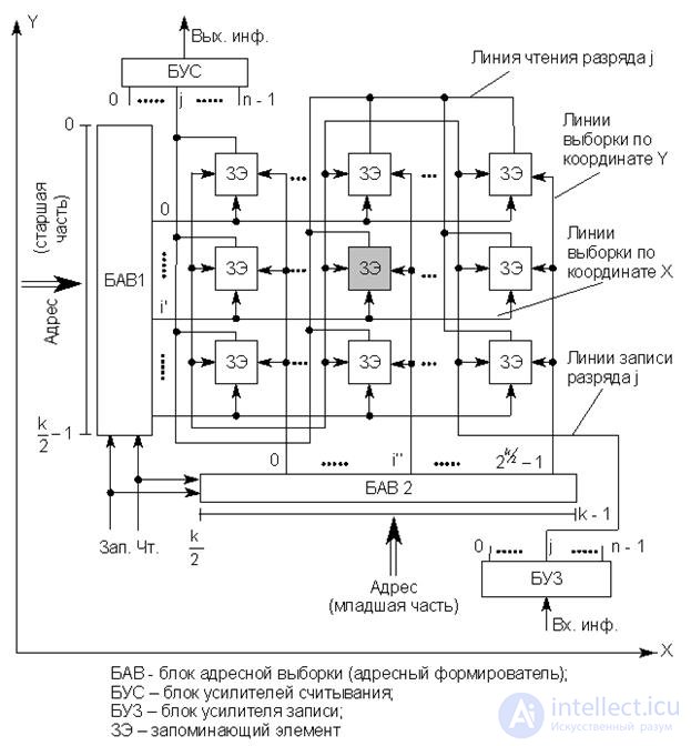
Fig.14.7. 3D type memory structure for j-th digit
The 3D type structure is the most convenient for constructing static memories on multiemitter bipolar transistors.
In the 2D-M ZM type memory for recording n-bit binary numbers, it consists of n flat matrices for the like digits of all numbers, which takes place in the 3D type memory. However, the process of writing and reading information is significantly different, since the memory of the 2D-M type uses different GE, each of which is approached only by two coordinate lines. The ZE of such chargers has two inputs (coordinate and recording) and one output, but usually their output is combined with the recording input.
The structure of a single-bit memory of type 2D-M (3M for the j-th digit of all memory cells) is shown in Fig. 14.8. 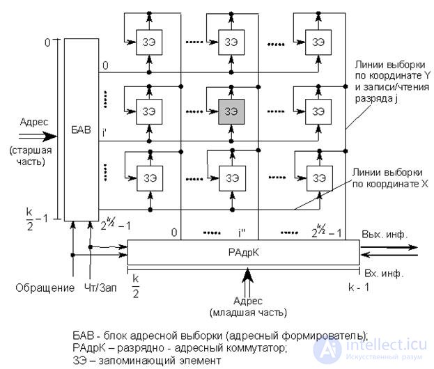
Fig.14.8. The structure of the memory type 2D-M for the j-th digit
As in the 3D type memory, the code of the address of the i-th memory cell is divided into two parts, one of which goes to the BAS, and the other to the bit-address switch (RADK). Radar is not only a device of address sampling of the j-th digit of the i-th memory cell, but also a device for recording and reading information stored in GE. If the BAS and RADC do not receive a memory access signal Obr, then the signals acting on the GE will not appear on their output lines and all GEs are in storage mode. In the presence of the signal Obr, read or write is performed depending on the signal of Th./App. When reading a BAS, it generates a sampling signal for reading along the i line, through which from all the EZ lines i ¢ the signals of their states are sent to the radar. The RADRK switch multiplexes these signals and sends to the output ( Output info ) a signal only from the i² line. When recording, the BAS generates a sampling signal for recording on line i. Switch RadrK depending on the value of the signal Bx. inf . outputs a recording signal 0 or 1 to the i² line and signals that do not affect the GE in other lines. As a result, the recording is made only in the GE, which lies at the intersection of the coordinate lines i and i², with i ¢ / i² = i (the gray earth).
The 2D-M type structure is the most convenient for building semiconductor chargers on MOS structures and is widely used nowadays in both dynamic operational and permanent memory.
Permanent memory in the operating mode of the computer can only read the stored information. Depending on the type of ROM, entering information into it is made either in the manufacturing process or under operational conditions by tuning, which anticipates the use of ROM in the computational process. In the latter case, the ROM is called permanent memory with variable in-use content or programmable permanent memory (PROM).
Permanent memory is usually built as an address. The operation of the ROM can be considered as the execution of a unique transformation of the k-bit code of the address of the cell of the storage array 3M to the n-bit code of the word stored in it.
Compared with random access memory, which allows both reading and writing information, the ROM design is much simpler, their performance and reliability are higher, and the cost is lower. This is due to the greater simplicity of the GE, the absence of circuits for writing in general or, at least, for real-time recording, the implementation of non-destructive readout, which excludes the information regeneration procedure.
One of the most important applications of ROM is the storage of microprograms in microprogram control devices of computers. For this purpose, the required ROM is much larger than in the OP, speed and moderate capacity (10 000 - 100 000 bits).
Permanent memories are widely used for storing programs in specialized computers, including micro computers, designed to solve a specific set of tasks for which there are well-established algorithms and programs, for example, onboard computers of airplanes, rockets, spacecraft, control computers, working in the process control system. Such an application of the ROM can significantly reduce the requirements for the capacity of the OP, increase reliability and reduce the cost of the computing installation.
ROMs are widely used in mainframe computers of all classes for storing standard procedures for initializing a computing system and external devices, for example, BIOS in an IBM PC. The software controllers of intelligent external computer devices are usually also stored in embedded ROMs.
In fig. 14.9 the scheme of the elementary ROM with structure of type 2D is resulted.
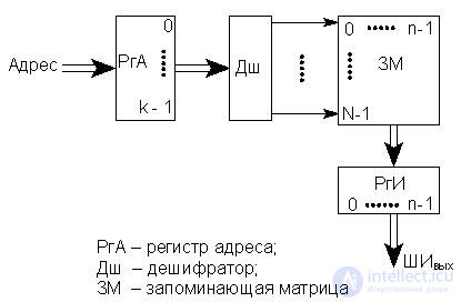
Fig.14.9. 2D 2D permanent storage
The storage array is formed by a system of mutually perpendicular lines, at the intersections of which GE are established, which either connect (state 1) or do not connect (state 0) between themselves the corresponding horizontal and vertical lines. Therefore, the ZE in the ROM is often called connecting elements. For some types of ZE, the state 0 means simply the absence of a storage (connecting) element in a given position of the MC.
The DSh decoder, using the address code in PrGA, selects one of the horizontal lines (one of the 3M cells) to which the sample signal is sent. The output signal (signal 1) appears on those vertical bit lines that are connected to the excited address line. Depending on the type of storage (connecting) elements, resistor, capacitive, inductive (transformer),
продолжение следует...
Часть 1 Theme 11. Storage devices Lecture 14
Часть 2 14.5. Flash memory - Theme 11. Storage devices Lecture 14

Comments
To leave a comment
Computer circuitry and computer architecture
Terms: Computer circuitry and computer architecture