Lecture
In order to optimize the operation of processors, a large number of auxiliary chipsets are produced, called chipsets, which perform any particular processor functions and / or act as a connecting component, ensuring the joint functioning of all computer components and devices built on their basis, for example cell phones. Further, the ideology of constructing support schemes for the MP will be examined on the example of chipsets for the x86 architecture used in personal computers like the IBM PC. Among the main producers of such chipsets are Intel, NVidia, AMD, Via, SiS.
Section 10 showed that the transition from mainframes to small computers (mini and micro) was accompanied by a significant simplification of the internal structure of the computer, namely, the transition to the main-modular structure. The main-modular structure assumes the presence in the computer of some common trunk, to which all the computer devices made in the form of functionally complete units are connected in the required nomenclature and quantity. This highway received the name of the system. Initially it was the only communication channel through which information was transmitted inside a computer between two or more components of the system. In the process of evolution of mini-and micro-computers, as well as increasing the speed of processors of a single system bus, it was not enough. However, the need for continuity of software and hardware of mass-produced computers of different generations did not allow to simply replace the previously developed system backbones with faster ones, although their performance did not match the performance of new generations of processors. A compromise solution to this problem turned out to be the introduction, in addition to the main system highway, of a number of other, more high-speed highways, which were called local tires . In the process of computer evolution, some of them lost their significance and disappeared (for example, VLB), others continued to develop, taking on more and more functions of the main system backbone (for example, PCI). Therefore, in addition to the main system bus, modern computers have a number of high-speed local buses for various purposes.
Before proceeding to the main stages of the evolution of the IBM PC bus architecture, it is necessary to make a number of observations. It has already been noted that various terms are used in the literature to refer to a system or a general highway. These are primarily the terms: "common bus", "system bus", "explosive bus" and "expansion bus". The latter term reflects the fact that the system bus allows you to connect additional PUs to the computer in order to expand or change its capabilities, i.e. allows you to change the hardware configuration. In this part of the explosive devices installed directly on the system (motherboard) and can not be replaced by the user, and part of the explosive devices placed in slots installed on the system trunk. When interacting with the MP, those and others use the same system backbone. The number of expansion slots may be different. There were five of them in the first IBM PC, and eight in the PC / XT. In subsequent PC models with high-speed local tires, their number changed depending on the specific configuration of the motherboard.
In the further presentation of the material, the term expansion bus (SR) will be used, since the system bus itself has already undergone significant changes in the first RS in comparison with the classical version of the structure of the simplest microcomputer shown in Fig. 13.1.
The performance of the SRs of the first IBM PC (8 MHz) was quite consistent with the speed of the I8088 processor, on the basis of which they were built. Meanwhile, to optimize the exchange process between the OP and MP, the developers went on complicating the PC structure and introduced two additional buses - a processor bus and a memory bus . Thus, the exchange inside the computer core (ie, between the OP and MP) was carried out not via SR, but through an autonomous highway consisting of two buses, which some authors call the local system bus . This term will be used in the further presentation of the material. The interaction of the processor bus and the memory bus, as well as their interaction with SR, was carried out through a set of specialized microcircuits (chipset), which can be conventionally called a bus controller . The very simplified structure of the tires of the first IBM PC is shown in Fig. 21.1
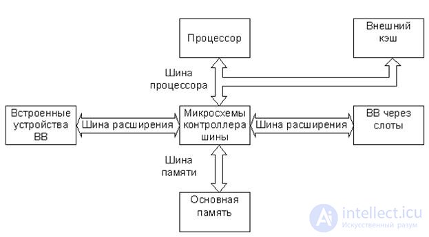
Fig.21.1. Simplified bus structure of the first IBM PC
The processor bus is the fastest and is designed to transfer data, commands, addresses and control signals between the MP and the bus controller, which connects it to the OP and SR. The processor bus of the first IBM PC worked at the same clock frequency as the processor, so the data word or address could be transmitted over it during one or two processor clock frequencies (in modern PCs, the processor bus clock frequency is always lower than the processor clock frequency). An external cache was connected to the same bus, which allowed the processor to exchange - the cache with the maximum speed. The number of physical circuits in the processor bus is significantly different for different generations of processors. So, in a computer with an I80286 processor, the processor bus had 24 address lines, 16 data lines and 12 control signal lines, and in a computer with a Pentium processor, there were already 32 address lines, 64 data lines, and almost three times more control line signals.
The data transfer rate on the processor bus (as well as on any other bus) is determined by the product of the bus width and the bus clock frequency divided by the number of clock cycles needed to transmit one bit. So, for the first models of the Pentium processor with a clock frequency of 66 MHz, coinciding with the clock frequency of the processor bus, the maximum data transfer rate is
66 MHz ´ 64 bits = 4224 Mbit / s ® 4224 Mbit / s: 8 = 528 MB / s.
It is assumed that the transfer of the computer word occurs in one period of the clock frequency of the bus. This data transfer rate is called bus bandwidth and is the maximum. It is always higher than the average working performance of the tire by about 25%. Thus, for the considered example, the average operating performance of the bus will be about 400 MB / s.
The memory bus is designed to transfer information between the OP and MP, as well as the OP and PU in the PDP mode. Information on the memory bus is transmitted at a significantly lower speed than the processor bus. This is due to the fact that the memory bus contains less data lines. Their number is determined by the width of the sample. In addition, as already noted, the speed of memory chips is always lagging behind the speed of the processor, so the process of transferring information through the memory and processor buses (that is, the local system bus) requires mandatory synchronization, which is performed by the bus controller. Already in the first models of the IBM PC, the OP was performed as separate modules (SIMM), which were placed in special slots located on the memory bus, similar to the slots on the SR. This principle is also preserved in modern PCs, although the slots and memory modules (DIMM) themselves have somewhat changed.
As already noted, SR allows MP and OP to interact with different PU. During the time that elapsed since the first IBM PC appeared, quite a few variants of SRs were developed, since the appearance of new high-speed generations of processors and PUs (especially video systems) required more productive SRs. Meanwhile, one of the main reasons holding back the intensive introduction of new SHRs was their incompatibility with the old standards, according to which many companies have already released hundreds of thousands of PC electronic components and which became completely unnecessary in the case of using new ShRs. In this connection, the evolution of SR occurs rather slowly, without sharp jumps. The following highlights the main points in the evolution of the IBM PC architecture.
The ISA (Industrial Standard Architecture) bus was used in the first IBM PCs built on the I8088 processor, in 1981. It had 8 data lines, 20 address lines, allowed to address up to 1 MB of memory and a clock frequency of 8 MHz. Data transfer required from two to eight cycles. The same SR was used in the next model - PC / XT, built on the I8086 processor.
The ISA bus is considered fairly simple, but IBM never published its full specification, so when creating adapter cards for the first IBM-compatible computers, developers had to figure out how to work themselves.
The appearance in 1984 of the second-generation I80286 processor, which already operates with 16-bit data, posed the problem of replacing or upgrading the SR-ISA. IBM went the other way, and a PC / AT computer appeared with dual expansion slots on an upgraded ISA bus. The second version of the ISA bus had 16 data lines, 24 address lines, allowing to address up to 16 MB of memory, and a clock frequency of 8 MHz. For data transmission also (as in the first version) it took from two to eight cycles. The first and second versions of the ISA bus were fully compatible, and dual slots made it possible to use old 8-bit adapter cards that could be inserted into the front of the slot. New (16-bit) adapter cards were inserted into both parts of the dual slot. The bandwidth of the new version of the ISA bus was
8 MHz ´ 16 bit: 2 clocks = 64 Mbit / s ® 64 Mbit / s: 8 = 8 MB / s.
Accordingly, the bandwidth of the first version of the ISA bus is half as much, i.e. 4 MB / s. As already noted, this is the theoretical, maximum data transfer rate. However, a rather complex exchange protocol significantly reduces the actual bus throughput. It is believed that the actual bandwidth of SR is about half of the maximum.
Subsequently, with the advent of 32-bit processors, some companies began to develop their own versions of the ISA bus expansion, but they did not receive any noticeable spread. Additional lines of these buses are usually used only when working with memory expansion cards and video adapters. Their parameters and wiring connectors are significantly different from the standard.
The appearance of the 32-bit I80386 processor led to the fact that the 16-bit ISA has ceased to correspond to the capabilities of the new generation of MPs. IBM did not begin to re-modernize the ISA bus, but developed a new one - the ISA (Micro Channel Architecture). The ISA bus is completely incompatible with the ISA bus and does not allow the use of old adapter cards, but in all respects it exceeds the 16-bit ISA bus. This is a rather expensive bus developed to peak with competitors for their PS / 2 computers, starting with model 50. The control signal composition, protocol and architecture are focused on asynchronous bus and processor operation, which eliminates the problem of matching processor and PU speeds. During operation, the ISA bus can transfer control to individual adapters connected to it ( bus mastering ), to implement the PDP mode or exchange between two adapters. All requests to seize the tire come in a specialized device called the bus arbiter (CACP - Central Arbitration Control Point). The arbitrator provides access to the bus to all devices in accordance with the priority system, preventing conflicts and monopolization of the bus by one of them. The bus architecture allows you to efficiently and automatically configure all devices programmatically (there are no switches on either the motherboard or on the adapters in the PSA / 2). There are 6 types of slots in the MCA bus:
- 16-bit;
- 32-bit;
- 16- and 32-bit with the addition of memory cards;
- 16- and 32-bit with additions for video adapters.
IBM wanted not only to replace the old ISA standard with a new one, but also to make money from it. IBM demanded that all manufacturers wishing to obtain a license to use the ISA bus pay for using the ISA bus in all previously released computers. This overwhelming demand led IBM’s competitor to develop an alternative EISA bus, which significantly slowed the spread of the ISA bus.
This reason, as well as the complete incompatibility with mass ISA-devices, led to the fact that the new ISA bus, despite the progressiveness of the architecture (relative to ISA), is not popular due to the narrowness of the range of users of MCA-devices. Meanwhile, the ISA still finds applications in powerful file servers, where it is necessary to provide highly reliable productive explosives.
EISA (Extended Industry Standard Architecture) appeared in 1988 in response to IBM’s development of the ISA bus and the requirement to license it. Competitors found it unnecessary to retroactively pay for the long-used ISA bus and, ignoring the new IBM development, created their own. Practically all leading manufacturers of computers (with the exception, of course, IBM) and the largest firms for the production of software products took part in this work. The first computers with an EISA bus appeared in 1989. This is the only highly standardized ISA extension up to 32 bits and up to eight expansion slots.
The EISA bus was developed as a successor of the ISA, and not as an alternative to it, so the differences between them are associated only with the appearance of additional capabilities. The EISA bus provides 32-bit slots for computers with 386DX processors and subsequent models. The EISA bus slot is designed in such a way that it allows the development of devices that have many of the capabilities of the ISA adapters, but it can also work with boards created in the old standard
darte isa.
Despite the significant increase in the number of lines in the EISA bus (55 new signals), the 32-bit EISA slot looks almost the same as the 16-bit ISA slot. Meanwhile, the slot EISA dual tires. Two rows of contacts correspond to the 16-bit ISA slot, the rest are located at the depth of the connector and relate to the expansion of the EISA, so the contacts of the edge connector of the old ISA boards that do not have a special key fall only on the top contacts of the slot.
Up to 32 bits of data can be transmitted over the EISA bus simultaneously at a bus clock frequency of 8.33 MHz. In most cases, data transmission takes place at least in two cycles, although a high transmission rate is also possible. Maximum bus performance is realized by burst mode - a high-speed mode of forwarding data packets without specifying the current address within the packet. In the packet, the next data can be transmitted in each bus cycle, i.e. The maximum throughput of the EISA bus is
8.33 MHz ´ 32 bits = 266.56 Mbit / s ® 266.56 Mbit / s: 8 = 33.32 MB / s.
The packet length can be up to 1024 bytes. Data transfer via "incomplete bus" (when working with 8- or 16-bit adapter cards in the ISA standard) is carried out at lower speeds, respectively.
In the EISA bus (as in the MSA), it is possible to transfer control of the bus from one of the adapter master cards ( bus mastering ) to implement the PDP mode or exchange between the two adapters. The work of adapters is coordinated by a device called a bus arbiter (CACP), which is sometimes also called a peripheral controller (ISP - Integrated System Peripheral). The arbitrator temporarily places the entire system at the disposal of one or another adapter card in accordance with the four-level priority system, arranged in the following order (in descending order):
- regeneration of memory systems;
- direct memory access (DMA);
- processor;
- bus adapter ( bus-master ).
EISA bus computers provide self-tuning for interrupts and adapter locations. In computers with an ISA bus and several adapter cards, if jumpers and switches are not properly installed, misunderstanding is almost inevitable. The EISA self-tuning program detects possible conflicts and configures the system to exclude them. However, the user himself can set the desired configuration using jumpers and switches, which is necessary, for example, in troubleshooting.
EISA is an expensive, but self-justifying architecture used in multiprocessor systems, on file servers, and wherever a highly efficient, reliable SR is required.
The above types of SR (ISA, MCA, EISA) have a common drawback - a relatively low speed. The speed and bitness of processors and memory chips (and, consequently, of the local system bus) increased, and the characteristics of SRs improved "extensively", mainly due to an increase in their bit depth. For a number of PUs, the speed of which is determined by the "human factor", for example, a keyboard, a mouse, and a high speed SR is not required. However, in the presence of PU such as hard drives, video systems, etc., the low speed of the SR has the most direct impact on the performance of the system as a whole. Проблема быстродействия ШР встала наиболее остро с появлением графических пользовательских интерфейсов, таких как Windows, при работе с которыми возникает потребность в передаче и обработке очень больших массивов данных.
Достаточно очевидным решением этой проблемы является осуществление обмена между наиболее быстродействующими ПУ и ядром ЭВМ не через ШР, а через дополнительную быстродействующую магистраль, выходящую непосредственно на шину процессора. В этом случае ПУ получают доступ к самой быстродействующей шине компьютера наряду с внешним кэш. Такая конфигурация получила название локальной шины расширения или просто локальной шины ( local bus ). Подключение локальной шины такого типа иллюстрируется упрощенной схемой на рис. 15.2.
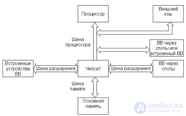
Fig.21.2. Simplified local bus connection
The first local bus appeared in 1992 as a result of the joint efforts of the companies Dell Computer and Intel. Although the system turned out to be quite expensive at first, it demonstrated the advantages of connecting the video system to the point where it was possible to take advantage of the high speed of the processor bus. This first version of the local bus was officially called the local I / O bus I486 (I486 local bus I / O). By the end of 1992, the cost of computers with a local bus began to decline, and many firms began producing similar systems.
To organize a local bus in a computer, it is not necessary to install expansion slots: an adapter for a device that uses a local bus can be mounted directly on the motherboard. In the first computers with a local bus, this option was used.
The local tire did not replace the previous standards, but supplemented them. The main expansion bus in the computer was still ISA or EISA, but one or several local bus slots were added to them. At the same time, compatibility with old expansion cards was maintained, and high-speed adapters were installed in the local bus slots, while realizing all their capabilities.
Компьютеры с локальной шиной стали особенно популярны среди пользователей Windows и OS/2, поскольку в слоты локальной шины можно было установить 32-разрядные платы так называемых видеоускорителей, которые значительно увеличивали быстродействие системы при работе с графическими изображениями. Производительность Windows и OS/2 существенно снижалась из-за ограничений, существующих даже в лучших платах VGA, подключаемых к шинам ISA или EISA. Обычные платы VGA могли выводить на экран до 600 000 точек в секунду, в то время как видеоадаптеры, соединенные с локальной шиной, по утверждениям изготовителей, за то же время выводили 50-60 млн. точек. В реальных условиях быстродействие, конечно, ниже, но разница все равно оказывалась существенной.
In its original version, the local bus slots were used almost exclusively for the installation of video adapters. By the end of 1992, several local tires were developed. Exclusive rights to them had only manufacturers. The lack of standards restrained the spread of local tires.
Приемлемое решение предложила ассоциация VESA (Video Electronics Standards Association), которая разработала конструкцию стандартной локальной шины, названной VESA Local Bus или просто VLB. Как и в первых конструкциях локальной шины, через слот VLB можно было получить непосредственный доступ к системной памяти, а ее быстродействие равнялось быстродействию самого процессора. По VLB можно было производить 32-разрядный обмен данными между МП и совместимым видеоадаптером, т.е. ее разрядность соответствовала разрядности данных процессора I80486. Максимальная пропускная способность VLB составляла
132 Мбайт/с.
Использование VLB позволяло изготовителям интерфейсных плат жестких дисков устранить еще одно ограничение: низкую скорость обмена данными между жестким диском и МП. Обычный 16-разрядный IDE-накопитель и его интерфейс могут обеспечить скорость передачи данных не выше 5 Мбайт/с, а адаптеры жесткого диска для VLB позволяли увеличить ее до 8 Мбайт/с. В реальных условиях пропускная способность этих адаптеров несколько ниже, тем не менее VLB существенно повышала быстродействие накопителей на жестких дисках.
VLB – стандартизованная 32-битная шина расширения, практически представляющая собой линии шины процессора I80486, выведенные на дополнительные слоты системной (материнской) платы. Конструктивно шина VLB выполнена в виде добавочных слотов, расположенных позади уже существующих системных слотов ШР ISA-16, EISA, МСА (по продольной оси) вблизи процессора. Таким образом, платы адаптеров одновременно вставлялись и в слоты ШР, и в слоты VLB. Слоты шины VLB обычно использовались для подключения графического адаптера и адаптера жесткого диска. Однако существуют системные платы, которые имеют встроенный графический и дисковый интерфейсы с шиной VLB, но сами слоты VLB отсутствуют. С точки зрения надежности и совместимости такой вариант наиболее оптимален, поскольку проблемы совместимости адаптеров и согласования нагрузок для шины VLB стоят очень остро.
При всех своих достоинствах шина VLB имеет ряд недостатков, основными из которых являются:
· Ориентация на процессор I80486. Уже отмечалось, что VLB является по существу продолжением шины процессора I80486, хотя возможно ее использование и с процессором I80386. Для процессоров Pentium была разработана спецификация 2.0 шины VLB, в которой число линий данных было увеличено до 64. Кроме того, спецификация включала аппаратный преобразователь шины Pentium в VLB. Однако дальнейшего развития эта версия не получила.
· Ограниченное быстродействие. Стандарт VLB допускает работу с тактовыми частотами до 66 МГц, но частотные характеристики разъемов VLB ограничивают ее на уровне 50 МГц. Если в компьютере установлен переключатель для повышения тактовой частоты процессора (например, для увеличения ее в два раза), то VLB продолжает использовать в качестве тактовой основную частоту МП.
· Схемотехнические ограничения. К качеству импульсных сигналов, передаваемых по шине процессора, предъявляются очень жесткие требования, причем они могут быть разными для различных типов ИС процессоров. Соблюсти их можно только при определенных параметрах нагрузки каждой из линий шины, т.е. к шине процессора должен быть подключен вполне конкретный "набор" элементов, например внешний кэш и ИС контроллера шины. При добавлении новых плат нагрузка на линии шины возрастает. Если не принять соответствующих мер, это может привести к искажениям импульсных сигналов ("звонам", завалу фронтов, изменениям логических уровней), а в результате – к потерям данных, нарушениям синхронизации и другим сбоям как самого процессора, так и адаптеров VLB.
· Ограничение количества плат. По указанным в предыдущем пункте соображениям количество одновременно используемых адаптеров VLB ограничено. Стандарт VLB допускает одновременную установку трех плат, но это возможно только при тактовой частоте до 40 МГц и малой нагрузке на шину. При ее увеличении и повышении тактовой частоты возможное количество адаптеров уменьшается. При частоте 50 МГц и большой нагрузке разрешается устанавливать всего одну плату VLB.
Указанные недостатки оказались настолько существенными, что в современных IBM PC шина VLB не используется.
В начале 1992 года на фирме Intel была организована группа, перед которой была поставлена задача разработать новую шину. В результате в июне 1992 года появилась шина PCI (Peripheral Component Interconnect bus), в апреле 1993 она была модернизирована. Ее создатели отказались от традиционной концепции, введя еще одну шину между МП и обычной шиной ВВ. Вместо того чтобы подключаться непосредственно к шине процессора, чувствительной к подобным вмешательствам
(о чем сказано выше), новый комплект ИС (чипсет) позволял создавать новую архитектуру шин IBM PC. Первые компьютеры с шиной PCI появились в середине 1993 года, и вскоре она стала неотъемлемой частью компьютеров класса high end.
Новая локальная шина существенно превосходила своих предшественниц по функциональным возможностям, производительности, надежности. Наличие чипсета делает шину PCI процессорно-независимой, что позволяет ее использовать с платформами не только на Intel-подобных процессорах. Это является очевидным преимуществом с точки зрения производителей плат расширения (адаптеров), которые стараются избегать разных версий одной и той же платы. Кроме того, наличие чипсета позволяет шине PCI работать параллельно с шиной процессора, не обращаясь к ней со своими запросами. Это даёт возможность процессору работать с данными, находящимися во внешнем кэш, в то время как по шине PCI может происходить обмен между ПУ и ОП в режиме ПДП (DMA).
Первоначально в IBM PC использовалась только версия 2.0 шины PCI, поддерживаемая чипсетами малой интеграции (5-6 микросхем) типа Neptun или Saturn. Однако с появлением чипсетов большей интеграции типа Intel 430 (Triton), Intel 440, Intel 810 в IBM PC стала использоваться новая версия шины PCI-2.1, которая вскоре была заменена версией PCI-2.2 (например, чипсет Intel 815). Эта версия используется и в настоящее время (чипсеты Intel 850, Intel 860, VIA KT 266 для процессоров AMD и др.). Версии 2.0, 2.1 и 2.2 имеют обратную совместимость на тактовой частоте 33 МГц. Основные возможности шины PCI следующие:
· Синхронный 32- или 64-разрядный обмен данными. Для уменьшения числа линий шины и контактов слота (а следовательно, и стоимости) используется мультиплексирование ША и ШД, т.е. для передачи адресов и данных используются одни и те же линии шины. Поддержка режима пакетных передач (linear burst), позволяющего не расходовать время шины на установку адреса каждого элемента данных при обмене блоком информации. Адрес автоматически модифицируется чипсетом для каждого последующего элемента данных. Это существенно повышает производительность шины при обмене ядра ЭВМ с видеосистемами и жесткими дисками большими блоками информации.
· Тактовая частота шины 33 МГц или 66 МГц (только для версий выше 2.0). Это позволяет обеспечить следующие максимальные пропускные способности шины с использованием пакетного режима:
ü 132 Мбайт/с при 32-бита/33 МГц;
ü 264 Мбайт/с при 32-бита/66 МГц;
ü 264 Мбайт/с при 64-бита/33 МГц;
ü 528 Мбайт/с при 64-бита/66 МГц.
· Работа на тактовой частоте 66 МГц возможна, если все адаптеры шины поддерживают эту частоту.
· Поддержка внешнего кэш с обратной и сквозной записью (write back и write through).
· Автоматическое конфигурирование карт расширения при включении питания.
· Полная поддержка режима multiply bus master, при котором на шине одновременно могут работать, например, несколько контроллеров жестких дисков.
· Установка запросов прерывания осуществляется по уровню (а не по фронту, как в шинах ISA и VLB), что делает систему прерывания более надежной и позволяет использовать одну линию прерывания для обслуживания нескольких ПУ.
· Спецификация шины позволяет комбинировать до восьми функций на одной плате (например, видео + звук + и т.д.).
· Шина позволяет устанавливать до четырех слотов расширения, конструкция которых существенно отличается от конструкции слотов шины ISA (EISA). Для увеличения числа подключаемых устройств (необходимость в этом возникает обычно в мощных серверных платформах) предусмотрено использование двух и более шин PCI, соединяемых одноранговыми мостами (peer-to-peer bridge). Следует отметить, что с разработкой нового поколения чипсетов (например, Intel 850, Intel 845, Intel 815, VIA KT 266 и др.) число слотов расширения, устанавливаемых на одной шине PCI, увеличилось до 5-6.
· Шина PCI имеет версии с питанием 5 В и 3.3 В. Разъемы для плат с питанием 5 В и 3.3 В различаются расположением ключей. Существуют и универсальные платы с переключаемым напряжением питания. Тактовая частота 66 МГц поддерживается только логикой питания 3.3 В.
· The PCI bus device has a timer used to determine the maximum time interval during which the device can occupy the bus when transmitting a block of information.
Considering the possibilities of the PCI bus, you need to keep in mind that the chipset is not just a matching element between different PC buses. It is the main link between all components of the motherboard. The set of tasks solved by him is very extensive and in many respects determines the characteristics of a specific computer model, therefore it is very difficult to consider the functionality of the PCI architecture in isolation from the functions of the chipset. For example, the ability to perform data exchange between the processor and the OP at the same time as the exchange between other PCI bus devices (concurrent PCI transferring) provided for in the bus specification is not implemented in all types of chipsets.
In general, the chipset can be divided into two functional parts. One part of the chipset allows the PCI bus to communicate with the local system bus (i.e., the processor bus and the memory bus). This part is called the main bridge ( host bridge ), north bridge (northbridge) or memory controller hub (Memory Controller Hub, MCH). The second part provides the interaction of the PCI bus with a hard disk, PSI cards and low-speed interfaces, such as SRA ISA, PCI Express, IDE, SATA, USB, etc. interfaces. This functional part of the chipset is called the PIIX bridge ( PCI, IDE, ISA Xcelerator bridge ), the south bridge (southbridge) or the I / O controller hub controller (ICH) . This functional division corresponds to the separation of the set of tasks solved by the chipset. Most often, the chipset of modern motherboards consists of two main microcircuits (MCH and ICH), but sometimes they are combined into one microcircuit (chip) and are called a system controller hub (System Controller Hub, SCH).
The functions of the main bridge include the following tasks:
· Maintenance of control and configuration signals of the processor.
· Multiplexing of the address and generation of control signals of the dynamic memory (OP), communication of the data memory bus with the local bus.
· Formation of control signals of the external cache, comparison of its tags with the current address of the address on the local bus (i.e., execution of functions of the cache memory controller).
· Ensuring coherence (reconciliation) of data in both levels of cache and memory when accessed by both the processor and the PCI bus device controllers.
· Communication of the multiplexed address bus and PCI bus data with the processor bus and the OP bus.
· Formation of control signals for the PCI bus, arbitration of the bus device controllers (i.e. performing the functions of the PCI bus arbiter).
· Support for AGP (Accelerated Graphic Port) backbone interface for connecting powerful graphics cards.
The PIIX bridge is also a multifunctional device and solves the following tasks:
· Organization of a bridge between PCI b buses, hard disk, PSI cards and low-speed interfaces, such as SRA ISA, PCI Express, IDE, SATA, USB interfaces, etc. with the coordination of the synchronization frequency of these tires.
· Implementation of standard system tools for BB - interrupt controllers, PDP controllers, system timer, speaker control channel, non-maskable interrupt logic, etc.
· Switching interrupt request lines of PCI buses and other buses, as well as embedded peripherals to interrupt controller request lines, managing their sensitivity (by differential or level), and coprocessor interrupt service.
· Switching channels PDP.
· Support for power saving modes.
· Implementing a bridge with an internal X-Bus bus used to connect keyboard controller chips, BIOS, CMOS RTC, floppy disk controllers and interface ports.
Chipset chips during initialization during initial testing (POST) are programmed in many ways, most of which are in the BIOS. Thus, motherboards made even on the same chipset can have different performance and ranges of supported installable components (processors, DRAM, cache). Accordingly, PCI buses implemented in various PC models (especially from different manufacturers) may differ somewhat in their functionality.
The very simplified IBM PC bus structure (considering the functions of the chipset) with the PCI bus is shown in Fig. 21.3.
The interfaces indicated on the diagram for connecting high-speed PUs (AGP, SCSI, IEEE 1394, IDE, USB) are not considered in this section. We only note that many models of modern IBM PCs have a number of other (not marked in the diagram) specialized interfaces for connecting various types of PUs.
For devices for industrial use in early 1995 was adopted standard Compact PCI, developed on the basis of version PCI 2.1. Compact PCI and PCI buses have electrical compatibility and the same bus communication protocols, although there are some differences in the system's autoconfiguration mechanism. Unlike the PCI standard, the Compact PCI standard allows you to install on one bus up to eight expansion slots, the design of which differs significantly from the design of the PCI slots and is designed for computer operation in harsh conditions - dust, vibration, humidity, etc.
In conclusion, it should be noted that the emergence of the PCI bus marked the beginning of the complete ousting from the IBM PC of the generally outdated SR-ISA. At present, the ISA bus has been almost extruded from the architecture of the IBM PC and all of its functions are performed by the PCI bus, which has evolved from a local to the main SR of a modern IBM PC.
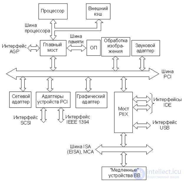
Fig.21.3. Simplified IBM PC bus structure
In this section, we briefly consider, for example, the three chipsets of different companies used in the construction of motherboards as of 2011. The architecture and functions of the chipsets are rapidly progressing, but the general solutions presented in Figure 15.3 still remain relevant. Structurally, part of the functions can be transferred to the processor, or both bridges can be implemented in one chip, but in most cases the chipset consists of two chips - the north bridge and the south one.
The functional diagram of the GeForce 9300/9400 chipset (another name is ION) is shown in Fig. 21.4.
Ion boards designed for building compact systems and netbooks. Obviously, in terms of supporting peripherals, all modern solutions in such conditions will be equal, and if someone is not able to provide a full-speed PCI Express 2.0 x16 slot, then nettop buyers will not be offended by it for it. The important features of the chipsets in this niche are as follows: processor support, memory support (type and maximum volume; the number of channels can also play a role due to the active reference of the graphics core to memory) and, of course, the integrated graphics.
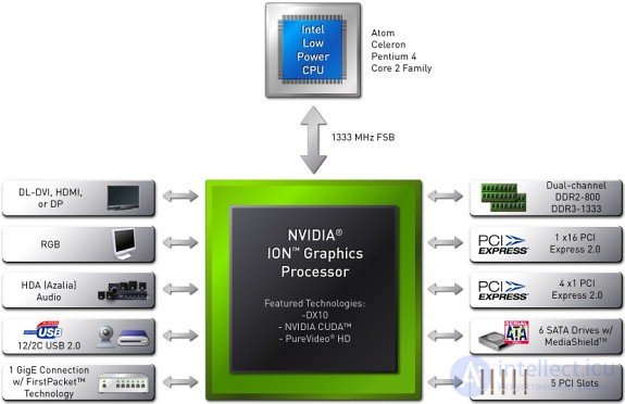
Fig.21.4. Functional diagram of the GeForce 9300/9400 chipset
ION has full hardware support for HD video playback and can output compressed or uncompressed 8-channel audio via HDMI, which makes it extremely attractive for use in media centers.
The functional diagram of the AMD 890FX + SB850 chipset is shown in Figure 21.5. 890FX - Northbridge IC, SB850 - Southbridge IC.
The specifications of the 890FX + SB850 chipset are as follows:
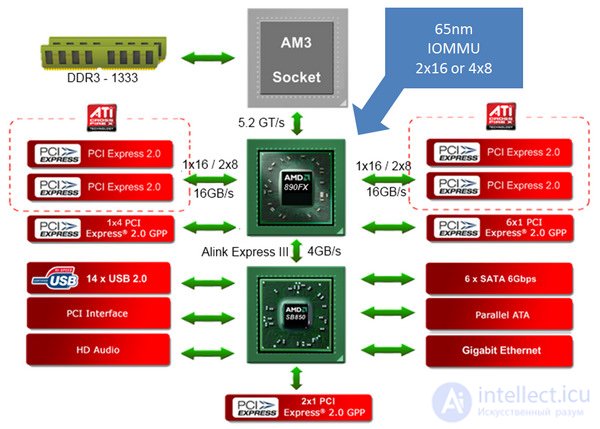
Fig.21.5. Functional diagram of the AMD 890FX chipset
The functionality of the Intel Z68 is as follows (Fig. 21.6):
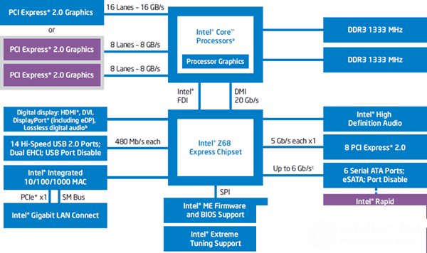
Fig.21.6. Intel Z68 Function Block Diagram
Z68 combined the advantages of the 6x series chipsets, while simultaneously supporting the integrated graphics of the new processors (output of a picture formed by the video core and sent over a special FDI interface to the display via a set of video outputs for every taste: HDMI 1.4, Display Port, DVI, analog d-Sub; two independent stream), the work of two video cards in x8 + x8 mode,
1. Simplified tire structure of the first IBM PC.
2. The evolution of the IBM PC expansion bus.
3. Simplified wiring diagram for local bus.
4. Local PCI bus.
5. Simplified IBM PC bus structure.
6. Functional diagram of the GeForce 9300/9400 chipset.
7. Functional diagram of the AMD 890FX chipset.
8. Block diagram of the functionality of the Intel Z68 chipset.

Comments
To leave a comment
Computer circuitry and computer architecture
Terms: Computer circuitry and computer architecture