Lecture
The element base of neural computing systems of the second and third directions (see part 1) are, respectively, custom crystals (ASIC), embedded microcontrollers (mС), general-purpose processors (GPP), programmable logic (FPGA - FPGA), transputers, digital signal processors (DSP) ) and neurochips [1]. Moreover, the use of both those and others makes it possible today to realize neurocalculators that function in real time, however, FPGAs, DSP, and of course neurochips found the greatest use in the implementation of neurocalculators.
As noted in [2], transputers (T414, T800, T9000) and, in particular, transputer-like elements are important for building computing systems with massive parallelism, and their use is gradually shifting towards switching systems and computer networks, although there are still examples of how to implement them layers of some computers with massive parallelism in the form of processor element lattices. More information about transputer systems and their application in building computing systems with massive parallelism can be found in [3].
DSP (Digital Signal Processor-Digital Signal Processor), having a powerful computational structure, allows you to implement various algorithms for processing information flows. The relatively low price, as well as advanced software development tools make it easy to use them when building computing systems with mass parallelism.
The rapid transition of modern control systems to digital standards has led to the need to process large volumes of information with high speed. Complicated processing and filtering of signals, such as unpacking compressed audio and video data, routing information flows, etc., requires the use of sufficiently productive computing systems. Such systems can be implemented on various components, but the most widespread devices are using digital signal processors and FPGAs.
Programmable logic can operate at higher frequencies, but since the control is implemented in hardware, changing the operation algorithms requires reprogramming the IC. The low DSP clock rate so far limits the maximum frequency of the processed analog signal to the level of 10-20 MHz, but software control makes it quite easy to change not only the processing modes, but also the functions performed by the DSP. In addition to processing and filtering data, DSPs can route digital streams, generate control signals, and even generate signals from the ISA, PCI system busses, etc.
It is customary to evaluate the speed of various devices based on DSP and FPGAs based on the execution time of typical digital signal processing operations (Sobel filter, FFT, Walsh-Hadamard transform, etc.). However, performance evaluations of neurocalculators use other indicators:
A feature of using DSP and FPGA as an element base for neurocalculators is that orientation in performing neural network operations causes, on the one hand, an increase in the exchange rates between memory and parallel arithmetic devices, and on the other hand, a decrease in the weight summation (multiplication and accumulation) due to the use of fixed a set of commands such as register-register [1-11].
For several decades, digital signal processors (DSP) have been the element base for building both neuroaccelerators and the logic of the system-wide control of neurocomputers. What kind of DSP can be used to implement neuro accelerators? - Yes, almost any, it all depends only on your imagination and capabilities, we will analyze only the MP of the three best-selling manufacturers: Analog Devices, Motorola and Texas Instruments, from the standpoint of building neural computing systems based on them.
The choice of a processor is a multi-criteria task, however, it should be noted that Analog Devices processors [7] are preferred for applications requiring large amounts of mathematical calculations (such as digital signal filtering, calculating correlation functions, etc.), since their performance is similar tasks higher than the processors of Motorola and Texas Instruments. At the same time, for tasks requiring intensive exchanges with external devices (multiprocessor systems, various controllers), it is preferable to use Texas Instruments processors [8], which have high-speed interface subsystems. Motorola is a leader in the production of signal microprocessors, most of which are cheap and reasonably productive 16-bit and 24-bit fixed-point microprocessors. Enhanced communication capabilities, the availability of sufficient amounts of intracrystal memory for data and programs, the ability to protect the program from unauthorized access, support for power saving mode make these microprocessors attractive for use not only as specialized calculators, but also as controllers in consumer electronic devices and systems adaptive filtering, etc.
The high performance required in real-time signal processing prompted Texas Instruments and Analog Devices to release transputer-like microprocessor families TMS320C4x and ADSP2106x, which are targeted for use in multiprocessor systems. Against this background, the first Russian signal processor (neuro-signal processor) from the Module company - "Neuro Matrix" [6], looks very worthy among the fixed-point DSPs. With a clock frequency of 50 MHz, the Neuro Matrix is practically not inferior in performance to products of world leaders, and even surpasses them in some tasks (Table 1) ["Electronics: science, technology, business" No. 2, 1999].
Tab. 1. Comparative tests of СISC processors, DSP TI and neural signal processor NM6403.
| The name of the test | Intel Pentium II 300 MHz | Intel PentiumMMX 200 MHz | TI TMS320C40 50 MHz | STC "Module" NM6403 40 MHz |
| Sobel filter (frame size 384X288 bytes), frames / s. | - | 21 | 6.8 | 68 |
| Fast Fourier transform (256 points, 32 bits), μs (cycles) | 200 | - | 464 (11588) | 102 (4070) |
| Walsh-Hadamard transform (21 steps, in. 5-bit data), s | 2.58 | 2.80 | - | 0.45 |
When creating neural computing systems based on signal processors, it must be remembered that DSPs have a high degree of specialization. They widely use methods for reducing the duration of a command cycle, typical of universal RISC processors, such as pipelining at the level of individual microinstructions and instructions, placing operands of most commands in registers, using shadow registers to save the state of calculations when switching context, and separating command and data buses (Harvard architecture). At the same time, for signal processors, the presence of a hardware multiplier, which allows multiplication of at least two numbers per command cycle, is characteristic. Another feature of signal processors is the inclusion in the command system of such operations as multiplication with MAC accumulation (C = AxB + C with the number of executions in the loop specified in the command and the rule for changing the indices of the used elements of arrays A and B, that is, preimages are already implemented basic neurooperations - weighted summation with accumulation), inversion of address bits, various bit operations. The signal processors implement hardware support for software cycles, ring buffers. One or more operands are retrieved from memory in a command execution loop.
The implementation of single-ended multiplication and commands that use the contents of memory cells as operands results in relatively low clock frequencies of the signal processors. Specialization does not allow to increase productivity due to the rapid execution of short commands such as R, R-> R, as is done in universal processors. These commands simply do not exist in digital signal processing programs.
Signal processors from different manufacturing companies form two classes that differ significantly in price: cheaper microprocessors for processing data in a fixed-point format and more expensive microprocessors that hardware support operations on data in a floating-point format.
Typical DSP operations require many simple additions and multiplications.
addition and multiplication require:
To select two operands in one command cycle, it is necessary to perform two memory accesses simultaneously. But in fact, besides sampling two operands, it is also necessary to save the result and read the instruction itself. Therefore, the number of memory accesses per command cycle will be more than two, and therefore DSP processors support multiple memory access during the same command cycle. But it is not possible to access two different memory addresses at the same time using one memory bus. There are two types of DSP processor architectures that allow implementing a mechanism for multiple memory access:
Harvard architecture has two physically separated data buses. This allows two memory accesses at the same time: Genuine Harvard architecture allocates one bus for selecting instructions (address bus), and another for selecting operands (data bus). But this is not enough for DSP operations, since basically all of them use two operands. Therefore, the Harvard architecture, as applied to digital signal processing, uses an address bus for data access. It is important to note that it is often necessary to sample three components — instructions with two operands, which the Harvard architecture itself is incapable of. In this case, this architecture includes a cache. It can be used to store those instructions that will be used again. When using the cache memory, the address bus and the data bus remain free, which makes it possible to select two operands. Such an extension — Harvard Architecture Plus Cache — is called the Extended Harvard Architecture or SHARC (Super Harvard ARChitecture).
Harvard architecture requires two memory buses. This greatly increases the cost of chip production. For example, a DSP processor operating with 32-bit words and in a 32-bit address space requires at least 64 pins for each memory bus, and a total of 128 pins are obtained. This leads to an increase in chip size and to difficulties in designing a circuit.
Von Neumann architecture uses only one memory bus. She has a number of positive features:
From the point of view of the implementation of neuro accelerators, we will focus only on some of the most prominent representatives of DSP, mainly belonging to the class of transputer-like DSP with floating arithmetic.
Realization of neurocalculators of high spatial dimension requires more and more efficient elemental base, to overcome the difficulties that arise, developers use two possible approaches: the first is to improve the performance of existing processors, and the second is to increase productivity by developing new architectures. The first method is limited to an increase in productivity of 5-8 times. The second method involves the development of architectures that would be most convenient in the final application and optimized for a particular programming language.
Analog Devices [7] is developing in both directions. So the core of the first 32-bit ADSP-21020 processor and the performance of 30 MFLOPS was improved, which led to the creation of the new ADSP-21065L processor with a maximum performance of 198 MFLOPS, which corresponds to an acceleration of 6.6 times. Working on a further increase in performance, optimizing the architecture of existing processors, a new signal microprocessor ADSP-2116x with a clock frequency of 100 MHz with a capacity of 600 MFLOPS was developed.
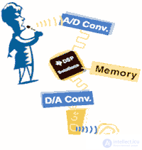
Fig.1.DSP is the basis of digital signal processing systems.
Among the main features of the ADSP-2116x DSP family are:
A universal processor ALU, a drum shift device and a universal multiplier function independently, providing a high degree of internal parallelism of operations. The general-purpose register file is used to exchange data between the computing modules and the internal bus, as well as to store intermediate results. The register file contains 32 registers (16 primary and 16 secondary), has 10 ports and, together with the Harvard processor architecture, allows you to organize an effective exchange between compute modules and memory. The extended Harvard processor architecture allows you to select up to two operands and a com *** y from the instruction cache in one cycle.
The ADSP-210xx processors contain a high-performance instruction cache. The cache works selectively: only those commands are cached, the selection of which conflicts with the selection of data from the program memory (PM).
Address generators (DAG1 and DAG2) provide a hardware implementation of cyclic (ring) buffers, allowing for efficient filtering and Fourier transform, which require a cyclic change in the addresses of the data being processed. The physically cyclic buffer can be located starting from any memory address, and register pointers are used to reference its contents. Two DAGs contain 16 primary and 16 secondary registers, which allows working simultaneously with 32 cyclic buffers.
Modern market requirements have led to the emergence of a new architecture, TigerSHARC, which, in order to obtain a high level of performance, combines many features of previously developed architectures. The new processor should combine the advantages inherent in existing DSP technologies, such as speed and certainty of command execution time, recognition of fast interrupts and high speed data exchange with peripheral devices.
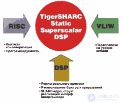
Fig.2. Principles of building architecture TigerSHARC
Для достижения наивысшей производительности ядра использованы особенности RISC архитектуры, такие как структура хранения и обмена данными и ком***ами, высоко конвейеризированный генератор адресов команд с возможностью предсказания переходов и объемным блокирующим файлом регистров. Также было решено взять в расчет особенности VLIW архитектуры для оптимизации построения команд. Полученная архитектура TigerSHARC достигает производительности 1.5 GFLOPS при 32-разрядных вычислениях с плавающей точкой и 6 GFLOPS при 16-разрядных с фиксированной точкой. Тактовая частота составляет на сегодня 250 МГц (рис.2.).
По данным компании Analog Devices [7] большинство нейросетевых реализаций на базе DSP схожи в использовании команд, но различаются набором данных. Особенно в многоканальных приложениях или в тех случаях, когда данные располагаются в виде прямоугольной матрицы, производительность может быть удвоена путем добавления второго набора математических модулей. Процессоры, содержащие второй вычислительный модуль, управляются также, как и небольшие SIMD-архитектуры. TigerSHARC позволяет использовать единственную ком***у для обработки данных в обоих вычислительных модулях - это уже элементы нейрочипа!
Более того, второй модуль может функционировать независимо от первого, для этой модели используются частично-множественные пути к данным. Для правильного выполнения команды в ней должно быть выделено дополнительное место, что приводит к очень длинным командным словам (VLIW - Very Long Instruction Word). Их использование приводит в большинстве случаев к быстрому заполнению небольшого объема внутрикристалльной памяти ком***ами NOP (no operation), которые предназначены для тех устройств, которые не будут задействованы в текущем цикле. Для избежания размещения команды NOP в коде в существующих VLIW разработках был найден большой недостаток, который был устранен делением длинных слов на более мелкие, параллельно поступающие к каждому устройству. Обработка множества команд независимыми устройствами одновременно является главной особенностью суперскалярной процессорной архитектуры.
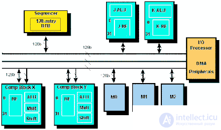
Fig.3. TigerSHARC Architecture
The heart of any processor is its computational subsystem. Each of the two computational modules, the Processing Element X (PEX) and Y (PEY), contains a 32-input 32-bit block register file in each input. At each calculation made by ALU, MAC or Shifter, the data will be selected from this register file, and then the results of calculations will be placed in it, which is the main feature of the read / write architecture (Fig. 3.). The use of a large number of registers for data storage simplifies the use of high-level programming languages. To achieve high internal bandwidth, each register file is connected to three 128-bit buses via two 128-bit buses.Both buses can be used simultaneously to perform read operations from memory and one bus can be used to write to memory. This bus structure defines typical mathematical instructions that require two data read operations and are downloaded by writing the result to memory.
Сравнительно большой объем внутрикристалльной памяти разделен на три независимых блока одинаковой величины. Каждый блок имеет ширину 128 бит, что соответствует четырехсловной структуре по четыре адреса в каждом ряду. Память может быть сконфигурирована по желанию пользователя без специальной сегментации на память программ и память данных. Для доступа к данным процессор может адресовать одно, два или четыре слова и передавать их в/из одно или оба вычислительных устройства за один такт. Кроме внутренней памяти архитектура TigerSHARC позволяет адресовать 4 ГСлов.
Одним из наиболее сложных устройств новой архитектуры является генератор адресов команд, определяющий порядок выполнения команд и отслеживающий правильность их выполнения в соответствующих модулях. Для снижения эффектов конвейеризации в нелинейном коде генератор адресов инструкций содержит буфер конечного перехода (Branch Target Buffer, BTB). Его механизм позволяет предсказывать переходы и сохранять их в буфере глубиной в 128-ячеек. С помощью предсказания переход может быть выполнен за один цикл вместо 3-6 без предсказания.
Объединение данных процессоров по любой из архитектур (кольцо, гиперкуб и т.п.), позволяет создавать полнофункциональные нейроускорители. Так, нейровычислительная сеть может быть выполнена в виде двумерного массива (в общем случае 4 ряда по высоте и n колонн) процессоров, подключенных к интерфейсным платам и с помощью хост-интерфейса к процессору общего управления. Каждый процессор в сети соединен с соседними, расположенными сверху и снизу относительно него, посредством четырех из шести имеющихся SHARC линков. Остальные линки процессоров используются для обеспечения частичного приема данных, необходимых в процессе вычислений. Архитектура обеспечивает масштабируемую сетевую процессорную модель с общей средой вычислений для каждого узла сети. Эта сеть подсоединяется посредством стандартного интерфейса разделяемой памяти к хост-процессору, который выполняет роль контрольного пункта системы.
Сигнальные процессоры компании Texas Instruments [8] разделяются на два класса: это процессоры для обработки чисел с фиксированной точкой и процессоры для обработки чисел с плавающей точкой (рис.4.). Первый класс представлен тремя семействами процессоров, базовыми моделями которых являются соответственно TMS320C10, TMS320C20, TMS320C50. Второй класс включает процессоры TMS320C30, TMS320C40, TMS320C80, которые поддерживают операции с плавающей точкой и представляют собой мультипроцессорную систему выполненную на одном кристалле, а семейство TMS320C6x включает как процессоры с фиксированной, так и с плавающей точкой.
Процессоры старших поколений одного семейства наследуют основные архитектурные особенности и совместимы "снизу вверх" по системе команд (чего нельзя сказать о процессорах, входящих в разные семейства). Процессоры компании Texas Instruments обладают высокоскоростными интерфейсными подсистемами и поэтому их предпочтительнее использовать для тех задач, в которых требуется выполнение интенсивного обмена с внешними устройствами (микропроцессорные системы, различного рода контроллеры).
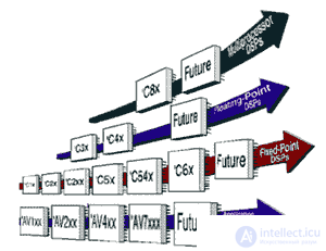
Fig.4. Иерархическое дерево микропроцессоров фирмы Texas Instruments [8].
Процессор TMS320C80 фирмы Texas Instruments с производительностью в 2 млрд. операций в секунду представляет собой комбинацию из пяти процессоров, реализованных по MIMD (multiple-instruction, multiple-data) архитектуре (рис.5.). На одном кристалле реализованы одновременно две технологии - DSP и RISC, расположены один управляющий RISC процессор и четыре 32-х разрядных цифровых сигнальных процессора усовершенствованной архитектуры с фиксированной точкой (ADSP0-ADSP-3), обладающие высокой степенью конвейеризации и повышенной до 64 бит длиной слова инструкций, а это в свою очередь позволяет описывать сразу несколько параллельно выполняемых команд. Каждый из процессоров работает независимо друг от друга и может программироваться отдельно друг от друга и выполнять различные или одинаковые задачи, обмениваясь данными через общую внутрикристалльную кеш-память.
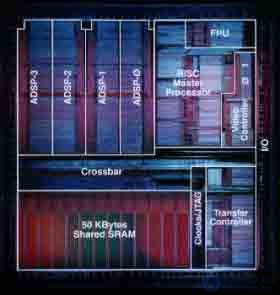
Fig.5. Размещение функциональных элементов TMS320C80 на кристалле.
Суммарная производительность TMS320C80 на регистровых операциях составляет 2 млрд. RISС-подобных команд в секунду. Благодаря столь высокой производительности TMS320C80 может заменить при реализации приложений более 10 высокопроизводительных ЦСП или ЦП общего назначения. Пропускная способность шины TMS320C80 достигает 2.4 Гбайт/с - в потоке данных и 1.8 Гбайт/с в потоке инструкций.
TMS320C80 обеспечивает высокую степень гибкости и адаптивности системы, построенной на его базе, которая достигается за счет наличия на кристалле параллельно функционирующих DSP процессоров и главного RISC-процессора. Архитектура процессора TMS320C80 относится к классу MIMD (Multiple-Instruction, Multiple-Data) - множественный поток команд, множественный поток данных. Входящие в состав TMS320C80 процессоры программируются независимо один от другого и могут выполнять как разные, так и одну общую задачу. Обмен данными между процессорами осуществляется через общую внутрикристалльную память. Доступ к разделяемой внутрикристалльной памяти обеспечивает матричный коммутатор (Crossbar), выполняющий также функции монитора при обращении к одному сегменту памяти нескольких процессоров.
Основные технические характеристики процессоров семейства 'C8x':
Главный процессор (MP) - это вычислительное устройство с RISC-архитектурой и встроенным сопроцессором для выполнения операций с плавающей точкой. Подобно другим процессорам с RISC-архитектурой, MP использует команды загрузки/сохранения для доступа к данным в памяти, а также выполняет большинство целочисленных, битовых и логических команд над операндами в регистрах в течение одного такта.
Вычислитель с плавающей точкой (Floating-Point Unit, FPU) конвейеризирован и позволяет одновременно выполнять операции над данными как с одинарной, так и с двойной точностью. Производительность устройства составляет около 100 MFLOPS при внутренней тактовой частоте 50 МГц. FPU использует тот же регистровый файл, что и устройство целочисленной и логической обработки. Специальный механизм отметок (Scoreboard) фиксирует занятость регистров и обеспечивает их бесконфликтное использование.
Основными компонентами MP являются:
Архитектура ADSP-процессоров TMS320C80 ориентирована для применений, связанных с графикой и обработкой изображений (где использование нейропарадигм даем наибольший на сегодня эффект). Она обеспечивает эффективное выполнение операций фильтрации и частотного преобразования, типичных для данных приложений. ADSP может выполнять за один такт одновременно операцию умножения, арифметико-логическую операцию (например, сдвиг-суммирование) и два обращения к памяти. Внутренний параллелизм ADSP позволяет обеспечить быстродействие свыше 500 млн. операций в секунду на некоторых алгоритмах.
ADSP манипулирует 32-разрядными словами, а разрядность команд составляет 64 бита. Процессор использует прямую, непосредственную и 12 видов косвенной адресации.
Архитектура ADSP характеризуется следующими параметрами:
The exchange controller (TC) controls the exchange of processors and memory both inside the chip (through the switch) and outside the chip, using interface circuits that support all common memory standards (DRAM, VRAM, SRAM) and allow for dynamic change. bus widths from 8 to 64. Using the priority discipline of servicing memory requests in DMA mode, TC allows you to exchange data without interrupting calculations at speeds up to 400 MB / s. The exchange controller supports linear and coordinate memory addressing for efficient exchange performance when working with 2- and 3-dimensional graphic images.
Most of today's well-known DSP-based neurocomputers are based on microprocessors of the TMS320C4x family. Due to its unique structure, these DSPs are widely used in multiprocessor systems and have practically supplanted the family of transputers previously produced in a number of European companies. The TMS320C4x processors are compatible with the command system with the TMS320C3x, but they have higher performance and better communication capabilities.
The central processor TMS320C4x has a conveyor case-oriented architecture. CPU components are:
The multiplier performs operations on 32-bit data in a fixed-point format and 40-bit data in a floating-point format, with multiplication performed per clock cycle (25 ns), regardless of the type of data and in parallel with data processing in other functional units of the microprocessor ( for example, ALU).
In one clock cycle, the ALU performs operations on 32-bit integer and logical and 40-bit data in floating-point format, including operations for converting data presentation formats. The microprocessor hardware supports the division of the division and extraction of square root. The drum shifter allows you to shift data left or right by a number of positions from 1 to 32 in one clock cycle. Two additional register arithmetic modules (Address Generation 0 and Address Generation 1) operate in parallel with the multiplier and ALU and can generate two addresses in one clock cycle. The processor supports relative base, base index, cyclic and bit-reverse addressing.
The primary register file is a multi-input file of 32 registers. All registers of the primary register file can be used by the multiplier, ALU, and as general purpose registers. Registers have some special functions. 8 additional registers can be used for some indirect addressing methods, as well as general-purpose integer and logical registers. The remaining registers provide system functions such as addressing, stack management, interrupts, display of processor status, block repetitions.
High-precision registers are designed to store and process 32-bit integers and 40-bit floating point numbers. Additional registers are available for both the ALU and for two modules of register arithmetic. The main function of these registers is the generation of 32-bit addresses. They can also be used as a cycle counter or as general purpose registers.
The processor-addressed space is 4G 32-bit words. On the chip there are two two-input RAM0 and RAM1 blocks of 4 KB each, as well as a two-input ROM block containing the boot program.
The instruction cache of a processor with a capacity of 128 32-bit words contains the most frequently used sections of code, which makes it possible to shorten the average instruction sampling time. High performance TMS320C40 is achieved through internal process parallelism and multi-bus processor organization. Separate buses allow simultaneous sampling of commands, data, and direct memory access.
More and more popular, including for neuro applications, the TMS320C6x processor family has a record performance of 1600 MIPS. Thanks to this, a fundamentally new look at existing communication and telecommunication systems is possible. High performance of microprocessors is provided by the new VelociTIT architecture with a very long command word (VLIW, Very Long Instruction Word). The architecture of Velociti is formed by a set of parallel processors that allow you to execute several instructions in one command cycle. It is this parallelism of the processor architecture that provides high performance.
A comparative assessment of the performance of the most widely used today in DSP Analog Devices and TI neuro-applications is given in Table 2.
Table 2. Comparative characteristics [7].
| Feature \ Processor | ADSP21061 | TMS320C40 / TMS320C44 |
| Instruction Execution Time | 20 ns | 33 ns |
| Peak MFLOPS | 150 Peak MFLOPS | 60 Peak MFLOPS |
| Price (10,000 pcs) | $ 49 | $ 176 ($ 99 w / C44) |
| Price / performance | 3.1 MFLOPS / $ | 0.34 MFLOPS / $ (.6 w / C44) |
| Benchmark: | ||
| 1K pt Complex FFT | .37 ms | .97 ms |
| Core Features: | ||
| Data registers | 32 | 12 |
| Circular buffers | 32 | 1 (Fixed Length) |
| I / O Capabilities: | ||
| DMA Channels | 6 | 6 |
| Serial ports | 2 with TDM mode | None |
| Max throughput | 300 Mbytes / sec | 60 Mbytes / sec |
| On-Chip Memory | 32K x 32 Bit Words | 2K x 32 Bit Words |
| Total On-Chip Memory Size | 1,024 Kbit (1Mbit) | 64 Kbits |
| Multiprocessing Support | 6 processors through cluster bus | 6 processors through COMM ports (4 processors w / C44) |
| Host interface | Parallel | None |
Motorola's signal processors are today to a lesser extent than those discussed above, are used to implement the neuroparadigm. They are divided into 16-bit and 24-bit fixed-point microprocessor families — DSP560xx, DSP561xx, DSP563xx, DSP566xx, DSP568xx, and floating-point microprocessors — DSP960xx. Motorola’s 24-bit microprocessor line includes two families: DSP560xx and DSP563xx. The fundamentals underlying the Motorola signal microprocessor architecture were developed and implemented in the DSP560xx family. Further work on the improvement of signal processors was carried out in three directions:
Motorola is a leader in the production of signal microprocessors, however, most of which are cheap and fairly high-performance 16-and 24-bit microprocessors with a fixed point. Enhanced communication capabilities, the availability of sufficient amounts of intracrystal memory for data and programs, the ability to protect the program from unauthorized access, support for power saving mode make these microprocessors attractive for use mainly as specialized computers, controllers in industrial robots, consumer electronic devices, weapon control systems, means of wireless communication, etc. Examples of building neurocalculators based on them are not known to us.
Separately, you should consider the possibility of creating parallel calculators (including neuro) based on FPGAs (programmable logic integrated circuits). Systems of both the second and third types can be implemented on the FPGA (see part 1), also recently, hybrid neurocalculators are widely used when the data processing unit is implemented on the DSP, and the control logic on the FPGA. Currently, many firms in the world are engaged in the development and production of various FPGAs, however, the leadership is shared by two firms Xilinx and ALTERA. It is impossible to single out the products of any one of these firms, since they differ very little in technical characteristics.
Currently, ALTERA manufactures seven families of VLSI FPGAs. The main characteristics of the most popular of them are given in table 3.
Table 3. Characteristics of FPGAs by ALTERA
| Specifications | VLSI families | |||
| MAX 7000E (S) | MAX 9000 | FLEX 8000A | FLEX 10K | |
| Architecture | Matrices AND-OR | matrices AND-OR | Conversion Tables | conversion tables |
| Logical capacity | 600-5000 | 6000-12000 | 2500-16000 | 10,000-100,000 |
| Inner memory | not | Not | Not | 6-24 Kb |
| The number of user pins | 36-164 | 60-216 | 68-208 | 59-406 |
Xilinx company produces seven series of FPGAs of two types:
Each series contains from one to several families, in turn, consisting of a series of crystals of different capacity, speed, body types.
The main features of Xilinx FPGA:
In the manufacture of FPGAs by Xilinx, three main technologies are used:
The implementation of FPGA-based neurocalculators requires the participation of an expert at the topological design stage. This is due to the fact that the automated mode of wiring does not yet allow to reach 60-100% of the use of crystal resources by wiring, and this is fundamental for tightly coupled schemes, which include neural network computers. Characteristics of the FPGA in terms of the implementation of neural network paradigms are presented in table 4 [10]:
Table 4. Features of the implementation of FPGA neurocalculators.
| No | Type FPGA | Manufacturer | Crystal complexity, macrocell (CLB) | Maximum number of neurons |
| one | XC4005E / XL | Xilinx | 196 (14x14) | 6 |
| 2 | XC4013XLA | Xilinx | 576 (24x24) | 18 |
| 3 | XC4020XLA | Xilinx | 784 (28x28) | 24 |
| four | XC4044XLA | Xilinx | 1600 (40x40) | 50 |
| five | XC4062XLA | Xilinx | 2304 (42x42) | 72 |
| 6 | XC4085XL | Xilinx | 3136 (56x56) | 97 |
| 7 | XC40250XV | Xilinx | 8,000 | 200 |
| eight | EPF10K2 | 0ALTERA | 144 | four |
| 9 | EPF10K50E | ALTERA | 360 | eleven |
| ten | EPF10K100E | ALTERA | 624 | nineteen |
| eleven | EPF10K250E | ALTERA | 1520 | 50 |
| 12 | M4LV-96/48 | AMD | 966 | 3 |
| 13 | M4LV-192/96 | AMD | 192 | 6 |
| 14 | M5LV-256 | AMD | 256 | eight |
| 15 | M5LV-512 | AMD | 512 | sixteen |
Building neurocalculators based on them, although it gives a high flexibility to the structures being created, it still loses in performance compared to other solutions.
The implementation of neural computing systems and specialized computing machines with mass parallelism based on DSP and FPGA is effective in solving problems of digital signal processing, video and audio data processing and building technical control systems. Comparative data on the implementation of FFT for DSP, RISC and CISC processors are given in Table 5 [9].
Table.5. Fourier transform execution time.
When implementing neurocalculators today, as a rule, the hybrid scheme is used with priority, when the block of matrix calculations is implemented on the basis of the cluster connection of DSP processors, and the control logic is based on the FPGA. The ADSP21060 and TMS320C44 are used as the element base of the matrix cluster, in the near future they will be replaced by the ADSP2106x and TMS320C67xx. In the future, the matrix core will be implemented on the basis of neurochips (the third part of the work will be devoted to review), and the signal processors and FPGAs will remain the basis for building control logic, which is already clearly seen on the neurocalculators known today, for example, Synaps 3, which the fourth part will be devoted to. articles.

Comments
To leave a comment
Computer circuitry and computer architecture
Terms: Computer circuitry and computer architecture