Lecture
It was noted earlier that in the course of evolution the classical computer structure underwent some changes, in particular, the memory device, the organization of which became hierarchical, changed. However, this is not all the changes that have occurred with the classical five-block computer structure and its basic principles of operation, formulated by von Neumann.
Below are very briefly considered some elements of the architecture of modern fourth-generation computers that go beyond the classical structures and principles of operation of the first computers of various classes. The material of the section, if possible, is illustrated by examples of constructing simplified elements of computing devices based on the I80386 processor, whose structures are fairly transparent.
One of the effective means of improving the architecture of modern computers is the tag organization of memory , in which each word stored in memory or register is tagged . The tag identifies the data type — integer, PRC, decimal, address, character string, descriptor, etc. In the tag field usually indicate not only the type, but also the length (format) and some of its other parameters. Tags are compiled. The format of the data stored in the memory, while having the form shown in Fig. 22.1.
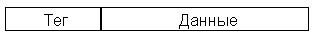
Fig.22.1. Tagged memory organization
The presence of tags attached to the data stored in the machine property of self-determination . This is a fundamental feature in the functioning of a computer.
It should be noted that computers with tag memory go beyond the model of the von Neumann computer as a result of the data self-determination. The classical von Neumann model is based on the fact that the type (character) of a given stored in memory is determined only in the context of program execution, or rather, the command that uses the given as an operand. In conventional computers corresponding to the classical von Neumann model, the type of data operands and their format are specified by the instruction's opcode, and in some cases the size (format) of the operands is determined by special command fields.
For example, in the IBM 360/370 command, the decimal addition by its opcode itself determined that its operands are decimal numbers. Special four-digit fields in this command set the number of decimal digits in the 1st and 2nd operands. Thus, IBM-360/370 had 256 codes of only one command decimal addition .
Tagged memory organization allows to achieve the invariance of commands regarding the types and formats of operands, which leads to a significant reduction in the set of machine commands. This simplifies and makes the processor structure more regular. In addition, such an organization of memory provides a number of advantages, namely:
- facilitates the work of the programmer, including when debugging programs;
- reduces the time spent on compilation (there is no need to select the type of command depending on the type of data);
- facilitates the detection of errors associated with incorrect setting of the data type (for example, when you try to add the address with the CHP).
Tagged memory organization contributes to the implementation of the principle of program independence from data .
And finally, something unexpected. The use of tags leads to savings in memory, despite the lengthening of the data format. This is due to the fact that in the programs of ordinary machines there is a large information redundancy on the specification of types and sizes of operands when they are used by several teams.
The disadvantages of such an organization of memory include some slowing down of the processor due to the fact that the establishment of correspondence of the command type to the data type in conventional computers is performed at the compilation stage, and when using tags is transferred to the program execution stage.
In the architecture of modern computers are also widely used descriptors - service words containing descriptions of arrays of data and commands. Descriptors can be used both in machines with tag organization of memory (for example, Elbrus computer), and without tags (for example, IBM computers on I80286 processors and later). In the latter case, limited self-determination of data is achieved.
The descriptor contains information about the size of the data array, its location (in the PD or the VI), the start address of the array, data type, data protection mode (for example, prohibiting writing to array cells) and some other data parameters that make it easier to work with arrays. So, setting an array size in a descriptor allows you to control the output beyond its boundary when indexing its elements.
As an example, consider one of the types of descriptors - a data descriptor in the B6700 machine of the Burroughs company (Fig. 22.2).
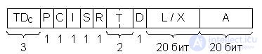
Fig.22.2. Computer Data Descriptor B6700 Burroughs, TDc - Descriptor Tag
The descriptor contains a specific TDc tag indicating that the word is a specific type descriptor, a group of pointers, and two fields A and L / X. The A field indicates the address of the beginning of the data array. Depending on the value of the pointer I, the descriptor describes the data array (I = 0) - and the length of the array L is placed in the corresponding field, or the array element describes (I = 1) - and then the index is in the field. This index indicates the offset of the element relative to the beginning array. Pointer P determines whether the array is in RAM or VP, i.e. it can be called the "Presence Indicator". In the latter case (being in the VI) field A indicates the location of the array in external memory. The remaining pointers have the following meaning:
D - single or double accuracy of data presentation;
T - describes a word or string;
R = 1 - data can only be read;
S - indicates the continuous or fragmented location of the array in memory;
C — Determines if the descriptor is a copy of another descriptor.
Intel processors, starting with the I80386 model, are equipped with means that allow implementing a mechanism for dividing the logical address space of memory into pages (4 Kbytes) and segments of different sizes (program, data, system segments, etc.). This issue is discussed in more detail in paragraph 16.4. All segments are treated as arrays, and descriptors are used to describe and address them. Each task can have a system and individual logical address space. These spaces are described by the global (GDT) and local (LDT) segment descriptor tables, each of which can contain a maximum of 8192 descriptors, respectively. In fig. 22.3 shows the format of the descriptors of the program segment and the data segment of the I80386 processor.
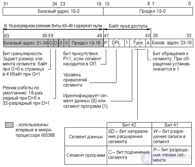
Fig.22.3. The format of the descriptors of program segments and data processor I80386
The assignment of descriptor fields is shown in Fig. 22.3, however some clarification is needed:
- "16-bit mode" is the full emulation mode of the I80286 processor.
- "Base Address" - a 32-bit field (of three fragments), defining the position of a segment in the address space of 4 GB.
- "Limit" - a 20-bit field (of two fragments), which determines the size of the segment. Depending on the value of the granularity bit G, the limit is calculated either in bytes (G = 0) or in 4 KB pages (G = 1). In the first case, the segment size does not exceed 1 MB, in the second it can reach 4 GB.
The use of descriptors in computer architecture implies that the access to information in memory is made through descriptors, which in this case can be considered as a further development of the device of indirect addressing. Addressing information in memory can be carried out using a chain of descriptors. In this case, multistage indirect addressing is implemented. Moreover, complex multidimensional data arrays (tables, etc.) are effectively described by descriptor tree structures. This can be illustrated by a simplified diagram in Fig. 22.4.
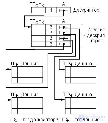
Fig.22.4. Description of a two-dimensional data array with a tree structure of descriptors
The terms "tag" and "descriptor" are widely used in technical literature when discussing issues of computer organization and computational processes. However, the interpretation of these terms in many cases is rather ambiguous, especially in the technical descriptions of specific processors and computers from different manufacturers, so you should always take into account the context in which these terms are used.
First, we will very briefly consider the reasons forcing engineers to continuously improve the hardware and ideological foundations of the data exchange processes between the processor and memory.
As already noted, the memory of modern computers has a hierarchical, multi-level structure. The higher the level, the higher the speed and the smaller the capacity. The upper level includes the memory with which the processor interacts directly during the execution of the program. This is, first of all, the main or RAM (OP), as well as super-operative internal memory of the processor. The latter has a very small capacity and will not be taken into account, i.e. it will be a question only of an exchange the processor - OP. The lower memory level includes external storage devices with high capacity and low speed. In all modern computers, the computational process is constructed in such a way that the number of calls to the EAP is minimal. In contrast to EPs, modern OPs have a fairly high speed (the circulation cycle is tens of nanoseconds or less). However, when organizing the interaction of the processor - OP there are many problems associated with the mismatch of the bandwidth of the processor and memory.
The continuous increase in performance (speed) of a computer, caused by the needs of their use, manifests itself primarily in increasing the speed of the processors. This is achieved using more high-speed electronic circuits, as well as special architectural solutions (pipeline and vector data processing, etc.). The speed of the OP is also growing, but all the time lags behind the performance of the processor hardware. This is primarily due to the fact that at the same time there is a rapid growth of its capacity, which makes it more difficult to reduce the cycle time of the memory.
The results, which leads to such a gap in the speed of the processor and OP, can be illustrated with a simple example. Consider a typical cycle of the microprocessor to the OP, consisting of a series of cycles T 1 T 2 ... T 5 , for example, MP KR580. In tact T 1 MP sets the address of the memory cell to SHA, which will be accessed. In T 2 MP, a READY signal is expected from the memory module. The number of cycles T 2 in the General case is not limited. The beat of T 3 occurs only after the receipt of the signal READY. From this example, it becomes clear why an increase in the clock frequency does not always lead to an increase in the speed of program execution, since the MP simply “treading water” waiting for an OP response.
From all this it follows that there are at least two directions to optimize the exchange processes of the processor and the OP.
The first direction is the improvement of their hardware base. But, as it turned out, in this area there are a number of serious obstacles, both technological and fundamental. One of them is related to the speed of propagation of an electrical signal in a conductor. With a low exchange rate, the signal lag is not noticeable. However, it becomes noticeable when these speeds increase to values proportional to
10 9 rev. / S. With a further increase in the frequency of calls, it becomes impossible to guarantee the correct operation of the OD, since the time for receiving data will significantly depend on their location in the OD.
The second direction is optimizing algorithms for interaction between the processor and RAM, which, of course, also require hardware support. Below, very briefly, the most common methods of this direction used in the creation of modern computers are considered.
Consider the basic principles of pipelining command execution loop procedures (machine runtime).
Earlier, when considering the principles of operation of CU processors, we already mentioned the conveyor method of executing micro-commands, when the procedure for executing the i-th micro-command in the ALU was combined in time with the procedure for calling from the control memory i + 1 micro-command. This principle applies to the execution of machine commands. Back in 1956, Academician S.A. Lebedev. proposed to improve the performance of machines using the principle of combining in time the individual stages of the working cycle , and implemented this principle in an M-20 computer in the form of parallel execution of an operation in an ALU and sampling the next command from memory.
In modern computers, various variants of the conveyor method for performing operations are widely used, which significantly increases their productivity. Without going into details, we will consider the simplest example of a pipelined way for the microprocessor to perform the addition operation of two operands located in the OP. To do this, two commands must be executed: 1st — calling the first operand in the accumulator; 2nd - call the second operand and addition. In the process of executing the 1st command, the MP resources can be used while waiting for an OP response (for example, in MP KR580, this is T T 2 of each engine cycle). For this, it is necessary that, instead of a passive standby, the MP initiates a new exchange cycle with the OP to call the 2nd command. According to the corresponding readiness signals of the OP, the 1st and 2nd cycles of accessing the memory are consistently terminated and an addition operation is performed. In this case, the time of each call to the PD is not reduced, but the total time for the execution of two commands is less due to their overlap in time. Practice has shown that the use of the pipeline in one form or another significantly increases the average exchange rate of the processor - OP. At the same time, naturally, the software and hardware of the computer as a whole (and not just one MP) becomes more complicated.
In general, the pipeline principle allows the processor to execute multiple instructions in parallel. However, in this case, as a single device, the processor can no longer function. The sequence of execution of each command is divided in the processor into basic operations. To perform the operations of each type are specialized actuators.
The most common method of pipelining is that during the execution of the previous command, a sample is taken from the memory of the next command. This achieves rational use of the bus operating time, which was wasted in the usual processor architecture, and reduces the duration of the program, although the duration of the execution of individual commands may even slightly increase.
The combination in time of the stages of the command execution cycle has long been widely used in processors, which in this case are a set of specialized execution units controlled by a single CU. So, for example, in the MP of the company Zilog Z80000 a six-speed conveyor is used, and the command execution cycle consists of six steps, respectively:
- command selection;
- decoding the command;
- calculating the address of the operand;
- sampling operand;
- actually perform the operation;
- memorizing the result.
When the execution of a specific step of the previous command ends in the pipeline, the corresponding execution unit is released and the same step of the next command can be started. In an ideal situation, the next team should arrive on the conveyor at the moment when the previous team leaves it. This corresponds to a six-fold increase in performance. However, when executing real programs, maximum performance is never achieved for a number of reasons. This is primarily:
- different durations of the command execution stages, which forces to choose the tact of the conveyor operation corresponding to the duration of the “slowest” stage execution. This leads to a certain increase in the duration of the execution cycle of an individual command (the time it takes for the command to pass through the pipeline) as compared to the potentially possible one;
- not every team uses all executive units, which requires additional time for the work of special switching circuits;
- violation of the sequence of execution of program commands, which occurs when there are control transfer commands or interrupts.
Violation of strictly sequential execution of program commands causes the need to clean the pipeline from the commands that started execution after the command that violated this sequence (pipeline braking) and refilling the conveyor with commands from a new program point (pipeline overclocking). Доля команд, на которых естественная последовательность выполнения программы нарушается, обычно составляет 15-30% от общего количества команд. При этом вызываемое процентное снижение производительности превышает вероятность их появления в программе.
Наличие команд передачи управления и, в частности, команд условных переходов оказывает самое существенное влияние на производительность конвейера команд, поэтому разработчики идут на существенное усложнение архитектуры процессоров в целях уменьшения этого влияния. Основные пути уменьшения влияния команд условных переходов на производительность конвейера команд состоят в следующем:
- прогнозировании направления перехода по косвенным признакам;
- одновременной обработке команд по обоим направлениям перехода (в более простом случае – создание очередей команд);
- выборе направления перехода на основании анализа статистики ранее совершенных аналогичных переходов в теле цикла;
- выборе случайного направления перехода;
- методе "отложенных переходов", при котором на этапе компиляции после команды условного перехода размещаются команды, не связанные с направлением перехода (число таких команд равно числу ступеней конвейера).
Для уменьшения влияния различной продолжительности этапов цикла выполнения команды на производительность разработчики искусственно увеличивают число ступеней конвейера, разбивая этапы на подэтапы, продолжительность выполнения которых примерно одинакова. Однако увеличение числа ступеней конвейера ведет к увеличению времени разгона, которое может существенно понизить общую производительность конвейера при обработке программ с короткими линейными участками. Виду этого число ступеней конвейера команд должно быть оптимальным.
Опыт построения конвейеров команд показывает, что полностью исключить влияние перечисленных выше факторов на производительность конвейера команд не удается. Максимальная производительность возможна только при обработке программ, имеющих длинные линейные участки, с использованием всех ступеней конвейера.
При рассмотрении метода конвейеризации обмена был проигнорирован тот факт, что реальные устройства ОП не допускают одновременного обращения к нескольким ячейкам (имеются в виду реальные БИСы памяти, охваченные общим полем адресов). Выйти из этого положения позволяет следующий метод.
Известны два основных метода расслоения памяти. Суть этих методов состоит в том, что память строится на основе нескольких модулей. Но в одном случае модули памяти имеют раздельные адресные пространства (независимая адресация), а в другом – модули охвачены общим полем адресов и образуют единое адресное пространство. Оба метода предложены достаточно давно, но широко используются и в современных ЭВМ, причем в ряде случаев совместно. Рассмотрим их очень коротко.
Метод 1
Метод разделения памяти на два модуля с независимой адресацией был предложен и опробован еще в конце 50-х гг. лабораториями Гарвардского университета. Один модуль памяти использовался для хранения команд программы, другой – данных. Оба модуля имели собственные контроллеры памяти и раздельные магистрали доступа. Такой принцип построения ОП оказался во многих случаях очень эффективным и был успешно использован при разработке компьютеров различного назначения. Возник даже термин "Гарвардская архитектура".
Этот принцип сохранен и в современных вариантах ЭВМ (процессорах) Гарвардской архитектуры. Он позволяет совместить во времени циклы обмена с обоими модулями памяти и оказывается эффективным при обработке любых типов программ. В настоящее время Гарвардская архитектура широко используется при построении кэш-памятей мощных процессоров.
Метод 2
В простейшем случае используют два модуля с "веерной" (чередующейся) адресацией, при которой смежные адреса информационных единиц, соответствующих ширине выборки (слово, двойное слово и т.д.), принадлежат разным модулям (т.е. четные адреса принадлежат одному модулю, а нечетные – другому). Это позволяет процессору инициировать второй цикл обмена до завершения первого, поскольку адреса лежат в разных модулях, либо обращаться одновременно двум устройствам к разным модулям памяти. В результате за счет перекрытия во времени обращений к разным модулям пропускная способность ОП в среднем повышается.
Следует отметить, что веерная адресация, как и конвейер команд, оказывается эффективной только при наличии в программе достаточно длинных участков с последовательным выбором команд, т.е. когда вероятность появления команд передачи управления мала. Выигрыш в быстродействии оказывается максимальным, когда необходимо осуществить множество последовательных обращений к ОП в ходе пакетных пересылок в режиме ПДП. В этом режиме в качестве параметров пересылки блока данных указывается начальный адрес и количество слов, подлежащих пересылке.
Двунаправленное расслоение ОП не может предотвратить появления циклов ожидания поэтому были разработаны системы с 4- и более кратным расслоением ОП, в которых контроллер памяти обеспечивает распределение последовательно вырабатываемых адресов между несколькими модулями памяти.
Проблема повышения пропускной способности характерна для всех уровней иерархии внутренней памяти ЭВМ. Наиболее остро эта проблема стоит перед разработчиками динамических ОП, которые благодаря максимальной информационной емкости и низкой стоимости занимают ведущее место в составе внутренней памяти компьютера. В последнее время предложен ряд вариантов ОП повышенного быстродействия. Это FPM, MDRAM, EDORAM, SDRAM, BEDORAM, RDRAM и многие другие типы памятей.
Методы повышения быстродействия таких памятей основаны на предположении о "кучности" адресов обращения к ОП, т.е. на предположении о том, что адреса последующих обращений к ОП, вероятнее всего, расположены рядом с адресом текущего обращения. Внутренние механизмы реализации этих методов схожи с механизмами конвейеризации процесса выполнения команд в процессоре, расслоения памяти, кэширования только на уровне отдельных БИСов и модулей памяти.
Суть этого метода состоит в том, что между процессором и ОП включаются дополнительные блоки буферных памятей относительно небольшой емкости, но имеющие быстродействие существенно выше, чем ОП. При обращении к таким памятям у процессора не возникает проблем с запаздыванием сигналов и уменьшением из-за этого скорости обмена. Как уже отмечалось, повышение быстродействия БИСов памяти сопровождается резким повышением их стоимости, поэтому доля буферной памяти в общем объеме небольшая, порядка 16-256 Кбайт на 4-8 Мбайт основной памяти. Сверхоперативная память, упоминавшаяся ранее, также является буферной, однако ее емкость очень незначительна (десятки слов) и в данном случае не учитывается.
В общем случае буферная память состоит из двух модулей: буферной памяти команд и буферной памяти операндов. Структура памяти в этом случае имеет вид, показанный на рис. 22.5. Такая схема буферизации ОП использовалась еще в мэйнфреймах 60-х гг.
Представленные буферные памяти в современных ЭВМ скрыты от программиста в том смысле, что он не может их адресовать и может даже не знать об их существовании, поэтому они получили название кэш-памятей (cache – тайник). Некоторые ЭВМ содержат объединенную кэш-память операндов и команд. Наличие кэш в общем случае не исключает присутствия в процессоре небольшой сверхоперативной памяти.
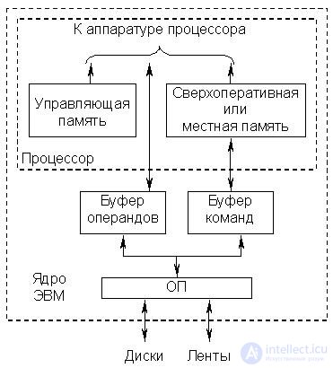
Рис.22.5. Схема подключения буферной памяти
Таким образом, кэш-память представляет собой быстродействующее ЗУ, размещенное в одном кристалле с процессором или же внешнее по отношению к кристаллу, но размещенное на той же плате. При обращении процессора к ОП для считывания в кэш пересылается блок информации, содержащий нужное слово. При этом происходит опережающая выборка, так как высока вероятность того, что ближайшие обращения будут происходить к словам блока, уже находящегося в кэш. Это приводит к значительному уменьшению среднего времени, затрачиваемого на выборку данных и команд.
Для обращения к кэш, размещенному вне кристалла процессора, но на одной с ним плате, может потребоваться несколько тактов, тогда как при обращении к кэш, размещенному внутри кристалла процессора, может оказаться достаточно одного такта. Однако даже размещение кэш на одной плате с процессором позволяет избежать большого числа циклов ожидания, которые неизбежны при работе с ОП, расположенной на отдельной плате и взаимодействующей с процессором через системную шину. Кроме того, выборка содержимого кэш-памяти может производиться произвольным образом, и, следовательно, в адресном пространстве кэш можно разместить командные циклы с входящими в них командами переходов (передачи управления).
All this allows not only to speed up the exchange of processor - memory, but also to reduce the load on the system trunk. The latter has become especially important with the emergence of multiprocessor systems in which processor elements are located on a common mainline and have a common OP module. It has already been noted that the exchange between computer devices over a common trunk is possible only at non-overlapping points in time (that is, only one processor can communicate with the OP at a time). Therefore, the cache memory turned out to be a very convenient tool for reducing the number of accesses of each processor to the RAM, and, consequently, the load on the computer system trunk.
Таким образом, снижение загрузки системной магистрали является еще одной причиной (помимо ускорения операций обмена процессор – ОП ) включения в структуру современных ЭВМ модулей кэш. Кроме того, наличие кэш-памяти достаточного объема позволяет не прерывать работу процессора даже при захвате магистрали каким-либо устройством, т.е. при осуществлении обмена в режиме ПДП.
Производительность кэш-памяти определяется временем доступа к ней и вероятностью удачных обращений , которая зависит от объема кэш и количества слов в блоке (строке), переносимых в кэш при каждом обращении к ОП. С увеличением длины блока возрастает вероятность того, что следующее обращение будет удачным, т.е. необходимая информация окажется в кэш-памяти. Однако эта зависимость нелинейная и имеет свой оптимум в координатах "производительность - стоимость", который обусловлен тем, что увеличение размера блока свыше некоторого оптимального приводит лишь к незначительному увеличению вероятности удачных обращений к кэш.
Полная производительность памяти ЭВМ (при наличии кэш) является функцией времени доступа к кэш, вероятности удачных обращений к кэш и времени обращения к ОП, которое происходит при неудачном обращении к кэш. Численная оценка полной производительности памяти оказывается в этом случае очень сложной задачей, особенно при учете увеличения быстродействия ОП за счет расслоения, и решается только статистическими методами.
При проектировании аппаратного и алгоритмического обеспечения кэш-памяти приходится учитывать большое число различных факторов и, часто взаимоисключающих, требований, поэтому конкретное исполнение кэш-памяти в различных ЭВМ отличается большим разнообразием. В частности, одной из проблем является взаимодействие кэш и ОП при изменении в процессе выполнения программы находящейся в кэш информации. В настоящее время эта задача решается, в основном, двумя путями, каждый из которых определяет тип кэш:
· Запоминание новой информации происходит одновременно в кэш и ОП (write through – сквозная запись ). При этом в ОП всегда есть последняя копия хранящейся в кэш информации. Это удобно, но длинный цикл ОП снижает производительность процессора.
· Запоминание новой информации происходит только в кэш. Копирование ее в ОП происходит только при передаче в другие устройства ЭВМ или при вытеснении из кэш в результате вызова новой информации из ОП (write back – обратная запись ).
Задача выбора алгоритма перемещения блоков информации из кэш-памяти в ОП при вызове из ОП новых блоков также не имеет однозначного решения. В большинстве случаев из кэш-памяти удаляется блок информации, который используется наиболее редко либо не использовался дольше других. Возможны и другие алгоритмы замещения. В частности, в кэш с прямым отображением, в котором за каждой ячейкой кэш закреплена определенная группа ячеек ОП, замена информации в ячейках кэш происходит по мере обращения процессора к соответствующей группе ячеек ОП (более подробно этот вопрос рассматривается ниже).
Следует отметить, что наличие кэш-памяти усложняет работу вычислительной системы и требует дополнительного программно- аппаратного обеспечения. В частности, требуется специальный контроллер кэш-памяти, который перехватывает обращения процессора к ОП и обрабатывает их непосредственно сам, без передачи запросов шине.
As an example, consider the organization of cache memory in computing systems built on the basis of a 32-bit I80386 processor. In the microprocessor architecture I80386, a sequence of eight contiguous bits is taken as a memory cell at the hardware level, i.e. 1 byte Despite the fact that the I80386 MP is 32-bit, the greatest efficiency is achieved in it when processing 16-bit data, therefore two combined bytes are chosen as the machine word in this MP.
In computing systems based on I80386, cache management is performed by a high-performance cache controller I82385. To initialize the I82385 controller, no special software is required, and the controller itself is software-invisible (transparent), so it can be easily applied to systems with already existing software, and the development of a new software product does not require specific conditions associated with this controller. The controller provides transparency on the tire by observing the tire ("eavesdropping" the tire). Monitoring of the bus is implemented by the controller through an interface similar to that of the I80386 processor bus. Due to its transparency, the I82385 cache controller can be incorporated into microprocessor-based systems based on I80386 for operation in pipeline and non-pipeline mode and for addressing OD space up to 4 GB. The OP update is performed on each write cycle using the write-through method. At the same time, performance improves due to issuing requests for write operations through some buffer, allowing the processor to continue working with the cache memory while the PD is being accessed. If the contents of the OP cells, copies of which are in the cache, have changed during the execution of the program, the controller automatically updates the contents of the corresponding cache cells.
The very simplified structure of the cache of the computing system based on I80386 and I82385 (yes, in principle, any other) is shown in Fig. 22.6. And in the computing systems based on I80386 and I82385, the combined instruction and data cache is used.
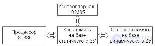
Fig.22.6. Cache organization
As already noted, the transfer of information from the OP to the cache and back is carried out in whole blocks. For this OP is also divided into blocks from 2 to 16 bytes. If the information requested by the processor is not in the cache, the cache controller updates the contents of the cache with the whole block. The block size is a very important parameter that determines the effectiveness of the cache. In 32 - bit systems, the controller sends a set of 2–4 words (4–16 bytes) as a block. Even if a single word is requested, block forwarding is still performed. As the block increases, the cache modification slows down, but the hit rate increases. Thus, increasing the block from 4 bytes to 8 increases the hit ratio by several percent. However, fewer blocks are placed in the cache. And with a decrease in the number of blocks, the probability of block transfers between the cache and the OD increases, so you have to choose the optimum (which has already been noted). Usually in computing systems based on I80386, I82385, the work of the cache memory is organized so that the probability of successful hits reaches 0.95.
When processing various classes of tasks, the highest efficiency of the cache memory system is achieved using different structures, namely: fully associative cache , forward mapping cache and multiple associative cache . Each of these structures has its own advantages and disadvantages. In principle, all these structures are supported by the I82385 cache controller with some limitations. Consider these structures in more detail, assuming that the capacity of the OP computer system is 16 MB.
· Fully associative cache (fig. 22.7)
The concept of a fully associative cache is based on the assumption that the processor accesses addresses located in different parts of the OD, so the cache mechanism must support multiple unrelated data blocks to ensure overall performance. Since there are no specific relationships between blocks in this case, the full address of each block and the block itself must be written to the cache. When accessing the memory, the cache controller compares the received address with the addresses mapped to the cache.
A significant disadvantage of a fully associative cache is that each time a memory is accessed it takes time to compare the addresses in the cache. It should be noted that in the standard configuration of computing systems based on the I80386 processor and the I82385 cache controller, the fully associative cache structure is not used.
Sequential comparison of cache cells with a 22-bit field of the feature (address) occurs without calling them to the controller. Such a consistent process of comparison and increases the search time.
It is also known that in a number of associative memory devices the association control is carried out sequentially on the bits of the associative feature. In relation to this cache, this means that a parallel comparison of 128 bits occurs in the i-th bit of the address, i.e. 22 comparisons must be performed in succession to analyze the entire field of the attribute (address). In specialized associative memory blocks, association control is performed in parallel across all memory cells.

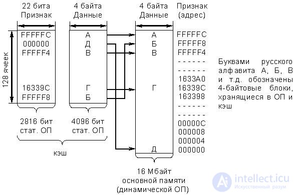
Fig.22.7. Fully associative cache organization
· Cache with direct mapping (Fig. 22.8)
When using a cache of this type of OP is divided into 256 pages by
64 KB each. Each page has its base address specified by 8 bits of the attribute field (high order bits of the OP cell address). The cache size (data bank) corresponds to the size of one page (64 KB). The index field in the address is 16 bits. Of these, 14 are used to select one of the 16 Kbyte 4 byte blocks (cells) cache or OP (on the page with the corresponding attribute), and two bits define one of the 4 bytes in the block, i.e. an index is nothing more than an offset from the base address (feature).

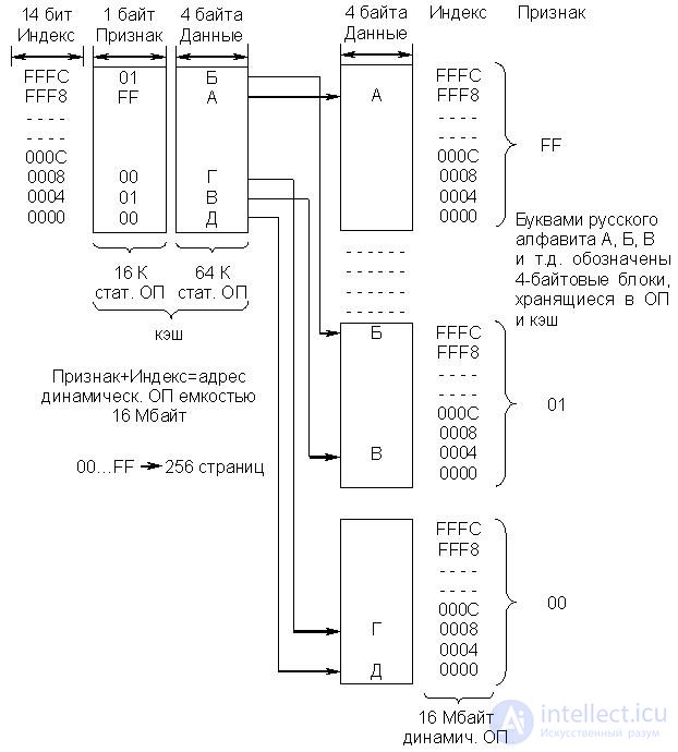
Fig.22.8. Organizing cache with direct mapping
Copies of blocks with the same addresses on all pages of the OD are placed in the same cache cell with the same address. Thus, 256 cache addresses are mapped to one cache address (256 * 64 KB = 16 MB). The cache itself has two levels. The first level is formed by a bank of signs and contains address information. In this case, these are the base addresses of the pages of the OP (features). In some sources, the term tag is used instead of the term. The second level consists of a data bank, which contains 4 byte copies (blocks) of the OP cells.
A simplified algorithm for processor accessing memory is as follows:
- The 14-bit index tells the cache controller which of the 16 KB single-byte cells in the feature bank should be checked:
- 8-bit sign, located in the specified cell of the bank of signs, reports which of the 256 possible 4-byte blocks is located at this address (index) in the cell of the data bank;
- if the feature requested by the processor matches the feature in the feature bank, a match has occurred. If not, the PD is accessed and the sign and data in the cache are replaced with data obtained from the PD.
The considered cache structure differs from the previous one (fully associative) in that there is no uncertainty in the allocation of the data block. The address (index) is specified directly in the processor request, and only the attribute has to be compared. This speeds up the exchange process.
The disadvantage of this type of cache is that 256 cache addresses are mapped to one cache cell, i.e. the same addresses from all pages of the OD, so when the processor cycles to the same addresses on at least two different pages, a "slip" cache occurs. In this case, on each access, the contents of the corresponding cache cell are updated.
This problem can be avoided by allowing any cell in the OP to be sent, as necessary, not to one , but to two or more cache cells. This increases the hit rate, but also complicates the algorithm for accessing memory.
· Two-input multiple associative cache (Fig. 22.9)
The multiple associative cache occupies an intermediate position between the fully associative cache and the cache with direct mapping. From the above structural scheme, it follows that the feature bank and the data bank used in the cache with direct mapping, in this case, are divided into two blocks, each of which has its own sign bank and a data bank with a capacity of 32 KB.
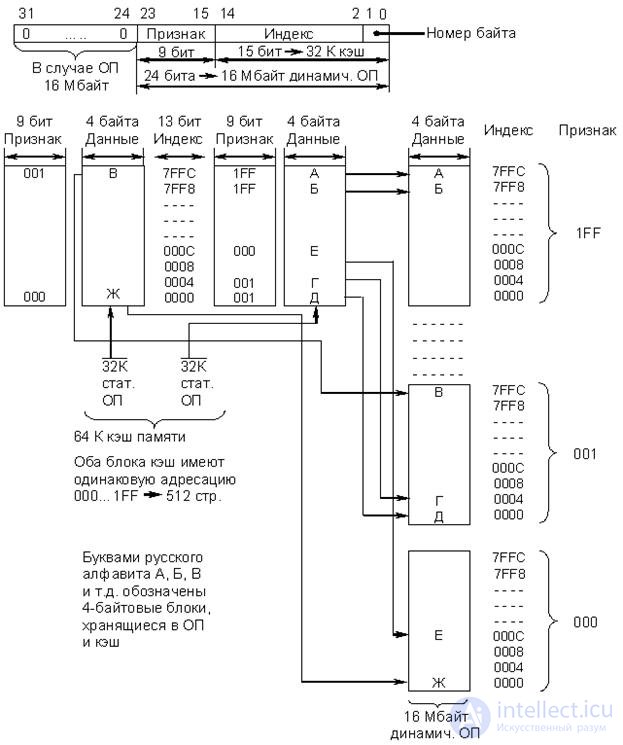
Fig.22.9. Two-way multiple associative cache organization
Both cache blocks have the same addressing, i.e. the index ranges from 0000 to 7FFC. When using this type of cache, the OD is no longer divided into 256 pages, but by 512, each of which has its own 9-bit flag (base address) from 000 to 1FF (32 KB). Data from the OP can be placed in any of the two cells with the corresponding index (offset) of the data banks belonging to different cache blocks. In accordance with the adopted algorithm, the cache controller I82385 places a new data block from the OD in that of the two cells whose contents have not been used for the longest.
The memory access algorithm is completely similar to that described earlier for a cache with direct mapping, except that in this case the controller has to simultaneously check two cells with the same indices (offset) in both cache blocks. The format of the address fields has also changed.
The performance for a dual-entry associative cache is about 1% higher than the cache with direct mapping. It is possible to build four-input or more multiple associative caches consisting of four or more blocks with the same addressing. This increases productivity, but also complicates the algorithm for accessing memory.
In conclusion, it should be noted that in computing systems based on the I80386 processor in the standard configuration, the cache controller I82385 supports the operation of a two-input multiple associative cache and a cache with direct mapping.
In modern computers, built on the basis of powerful processors, there is a further separation of internal memory and, above all, cache separation. High-speed first-level on-chip cache and a slower external second-level cache are essential components of all modern IBM PCs. The interaction of the cache of both levels is based on the principles similar to the principles of interaction of the remaining hierarchical memory layers - minimizing the number of hits of the faster layer to the less fast layer. A further increase in processor performance will inevitably entail a further stratification of the computer's cache memory.
In many cases, large executable programs and data structures cannot be fully accommodated in the OD, since the capacities of existing ODs are limited. This problem is especially acute in multi-program, multi-user systems that, roughly speaking, run several programs at the same time. Naturally, at each time point, the computer executes the command of a single program. However, whenever the processor's execution of a certain program is suspended due to the need to perform, for example, an explosive operation, the processor proceeds to process another program that is ready to run. It is assumed that at the same time in the OP there are several programs that can be in the active state, the state of readiness or waiting. However, there is no fundamental need for all programs (or one large program) to be in the EP, since at any given time the program concentrates on certain, relatively small areas. Thus, in the OP should be stored only used in this period of the program, and unused parts (programs or programs) can be stored in the external computer memory (VP).
When entering a computer into a computer, the user does not know, in combination with which programs his program will run, what place in the memory the operating system will allocate to it, therefore, when preparing programs, conditional addresses are used (preparation - this is the compilation operation of the program). Later, during the execution of the program, the operating system allocates space in the active parts of the program, and the conditional addresses are transferred to the executive . This procedure is called dynamic memory allocation .
The implementation of a dynamic distribution in a purely software way would lead to a significant loss of computer time, so hardware is also used for this purpose.
The most common method of dynamic memory allocation is based on the use of basic registers. The operating system assigns its base address to each user program. The base addresses of the processed programs are in the general registers of the processor. When executing a program, a physical address is formed by summing up the base and relative addresses. When dynamically allocating memory using basic registers, a program (or at least that part of it, whose addresses are converted using the same base address) must be located in consecutive cells and entered into the OT as a whole, although in the next cycle of activity it may be necessary just a small piece of the program.
With the considered method of dynamic memory allocation, free memory may consist of disconnected areas (memory fragmentation ) and a shift in the memory contents may be required to enter the desired program. This can be illustrated by an example on
rice 22.10.
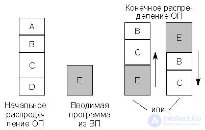
Fig.22.10. Memory allocation example
Initially, the OP is distributed between programs A, B, C, D. Programs A and D are currently the least active and can be considered as candidates for deletion to external memory. If the newly entered program E is more than any of programs A and D, then for its placement in memory it is necessary to shift programs B and C "up" or "down." This movement is associated with loss of time. Moreover, in a number of previous operating systems, such a move required the re-operation of editing links in the program and a new program load.
The noted deficiencies in the distribution of the OD are absent in virtual memory with paged organization.
The principle of virtual memory assumes that the user, when preparing his program, is dealing not with a physical EP, actually working as part of a computer and having some fixed capacity, but with a virtual (that is, seeming) single-level memory whose capacity is equal to the entire address space defined the size of the address fields in the formats of commands and basic registers. For example, the I80386 processor can manage virtual memory up to 64 TB (terabyte). This is a potential amount of virtual memory that can be controlled by a processor with a 32-bit EL. Meanwhile, the amount of virtual memory of real computers is significantly less than the potential. It is determined by the volume of the VP (hard disk), or rather the part that the operating system allocates for implementing the virtual memory mechanism. The amount of RAM in this case is not taken into account, since it is significantly less than the allocated amount of disk memory (VP).
The user has at his disposal the entire address space of the computer, regardless of the amount of its physical memory (RAM) and the amount of memory needed for other programs involved in multiprogramming. At the same time, flexible dynamic memory allocation is achieved, its fragmentation is eliminated, and considerable convenience for the programmer’s work is created. In modern computers, all this is achieved without a noticeable decrease in computer performance, at the cost of complicating the hardware, the operating system and the processes of their operation.
At all stages of program preparation, including loading into the OP, the program is presented in virtual addresses , and only at the execution of the machine command itself is the conversion of virtual addresses into real addresses of physical memory of a computer (they are also called physical addresses or executive addresses ).
The conversion of virtual addresses into physical ones is simplified, and the fragmentation of memory is also eliminated if the physical and virtual memory is divided into small blocks containing the same number of bytes. Such blocks are called pages . Pages of virtual and physical memory are assigned numbers, called numbers of virtual and physical pages, respectively. Каждая физическая страница способна хранить одну из виртуальных страниц. Нумерация байт в виртуальной и физической страницах сохраняется одной и той же.
Вновь загружаемая в ОП программа может быть направлена в любые свободные в данный момент физические страницы, независимо от того, расположены они подряд или нет. Не требуется перемещения информации в остальной части памяти. Страничная организация позволяет более рационально осуществлять обмен информацией между ВП и ОП, так как страница программы не должна загружаться до тех пор, пока она действительно не понадобится (имеется в виду, что обмен небольшими блоками информации между ВП и ОП можно осуществить без заметного снижения производительности процессора). Сначала в ОП загружается начальная страница программы, и ей передается управление. Если в процессе обработки программы делается попытка выборки слов из другой страницы, то производится автоматическое обращение к операционной системе, которая осуществляет загрузку требуемой страницы. Так происходит в процессе выполнения всей программы, при этом ненужные модифицированные страницы программы перемещаются из ОП в ВП. Операция замены (замещения) страниц в ОП называется свопингом (swapping), а часть диска, выделенная на нужды виртуальной памяти, – файлом подкачки (swap file). Размер этого файла, а следовательно, и максимальный объем виртуальной памяти конкретной ЭВМ зависят от общего объема жесткого диска и типа установленной операционной системы.
Соответствие между виртуальными и физическими памятями устанавливается страничной таблицей , причем физические страницы могут содержаться в текущий момент времени как в ОП, так и в ВП.
Упрощенная схема страничной организации памяти изображена на
rice 22.11.
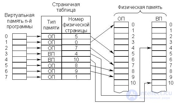
Рис.22.11. Упрощённая схема страничной организации памяти
Страничная таблица для каждой программы формируется операционной системой в процессе распределения памяти и перерабатывается ею каждый раз, когда в распределении памяти производятся изменения. Процедура обращения к памяти состоит в том, что номер виртуальной страницы извлекается из адреса и используется для входа в страничную таблицу, которая указывает номер соответствующей физической страницы. Этот номер вместе с номером байта, взятым непосредственно из виртуального адреса, представляет собой физический адрес, по которому происходит обращение к ОП. Процесс формирования физического адреса можно изобразить схемой, представленной на рис. 16.12, причем под номером физической страницы понимается ее базовый адрес.
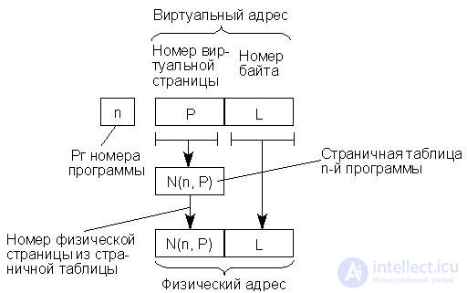
Рис.22.12. Формирование физического адреса
Если страничная таблица указывает на размещение требуемой информации во внешней памяти (ВП), то обращение к ОП не может состояться немедленно, так как операционная система должна организовывать загрузку в ОП из ВП нужной страницы.
Для каждой из программ, обрабатываемых в мультипрограммном режиме, организуется своя виртуальная память и создается своя страничная таблица, при этом все программы делят между собой одну физическую память (ОП и ВП).
Страничные таблицы программ хранятся в ОП, и обращение к нужной строке активной страничной таблицы в ОП происходит по адресу , который определяется номером активной программы и номером виртуальной страницы.
Следует иметь в виду, что механизм организации страничной адресации в реальных вычислительных системах, даже на процессорах поколения I80386, существенно сложнее описанного выше. В частности, для обращения к страничной таблице соответствующей программы операционная система должна первоначально обратиться к каталогу, в котором хранятся базовые адреса страничных таблиц соответствующих программ. Перемещение модифицированных страниц из ОП в ВП в большинстве случаев осуществляется не напрямую, а через кэшированную область ОП (дисковый кэш), поскольку велика вероятность обращения к недавно удаленной странице. Такой механизм позволяет ускорить процесс подкачки страницы при повторном обращении.
Для ускорения преобразования адресов обычно используется небольшая сверхоперативная память, куда передается из ОП страничная таблица активной программы. Кроме того, во внутренней памяти процессора обычно формируется сводная таблица, содержащая сведения о номерах виртуальных и соответствующих физических страниц для нескольких недавно использовавшихся страниц, в том числе принадлежащих разным программам. Так, внутрикристальный кэш процессора I80386 содержит информацию, необходимую для доступа к 32 страницам памяти, к которым недавно выполнялось обращение. В этом варианте сверхоперативная память, используемая при преобразовании адресов, строится как ассоциативная . Обращение к ней идет не по адресу, а по содержанию хранимой в ячейке информации – номеру программы и номеру виртуальной страницы.
До сих пор предполагалось, что виртуальная память, которой располагает программист, представляет собой непрерывный массив с единой нумерацией байтов. Такое логическое адресное пространство называют еще плоским или линейным . Между тем программа обычно состоит из нескольких массивов-подпрограмм, одной или нескольких секций данных. При программировании длина таких массивов (программных модулей) получается произвольной (различной), поэтому удобно, чтобы каждый массив имел свою собственную нумерацию байтов, начинающуюся с нуля . Желательно также, чтобы составленная таким образом программа могла работать при динамическом распределении памяти, не требуя от программиста усилий по объединению различных ее частей в единый массив. В современных вычислительных системах эта задача решается путем использования особого метода преобразования виртуальных адресов в физические, называемого сегментно-страничной организацией памяти.
Виртуальная память каждой программы делится на части, называемые сегментами , с независимой адресацией байтов внутри каждой части. При этом к виртуальному адресу добавляются дополнительные разряды левее номера страницы. Эти разряды определят номер сегмента.
Возникает определенная иерархия в организации программ, состоящая из четырех ступеней: программа-сегмент-страница-байт. Этой иерархии программ соответствует иерархия таблиц, служащих для перевода виртуальных адресов в физические. Программная таблица для каждой программы, загруженной в систему, указывает начальный адрес соответствующей сегментной таблицы. Сегментная таблица перечисляет сегменты данной программы с указанием начального адреса страничной таблицы, относящейся к данному сегменту. Страничная таблица определяет расположение каждой из страниц сегмента в памяти. Страницы сегмента могут располагаться не подряд – часть страниц данного сегмента может находиться в ОП, остальные во внешней памяти.
Следует отметить, что страничная организация памяти, сегментация памяти и разнообразные их комбинации и сочетания возникли в ранних универсальных вычислительных машинах, таких как IBM 360/370. В РС механизм сегментно-страничной адресации появился существенно позднее. Первыми процессорами фирмы Intel, имеющими аппаратную поддержку механизма сегментации памяти, являлись процессоры I80286. Однако наиболее широко защищенный режим (многозадачность, виртуальная память) стал использоваться с появлением 32-разрядных процессоров, в частности процессоров I80386, имеющих аппаратную поддержку механизма сегментно-страничной организации памяти. Такая поддержка позволила разработчикам системного программного обеспечения строить логическое адресное пространство памяти в соответствии с потребностями, определяемыми функциональным назначением ЭВМ. Процессор I80386 может работать как в реальном, так и защищенном режимах и поддерживает следующие варианты логической организации памяти:
- плоское (линейное) логическое адресное пространство, представляющее собой массив байтов со сплошной нумерацией;
- сегментированное логическое адресное пространство, состоящее из некоторого числа сегментов, каждый из которых содержит переменное число байтов;
- страничное логическое адресное пространство, состоящее из большого числа страниц, каждая из которых включает фиксированное число байтов;
- сегментно-страничное адресное пространство, состоящее из некоторого числа сегментов, которые, в свою очередь, состоят из целого числа страниц.
Процессор I80386 поддерживает 16000 сегментов различного объема. Размер каждого сегмента может достигать 4 Гбайт, что позволяет реализовывать управление виртуальной памятью емкостью до 64 Тбайт (в многозадачном режиме 16000 сегментов – для каждой новой задачи).
Перечисленные возможности позволяют программисту, в случае необходимости, использовать защищенный режим и разбить виртуальную память ЭВМ на сегменты. При этом каждому модулю программных кодов можно присвоить свой собственный логический сегмент памяти. Пользуясь моделью сегментной адресации, программист может разделить логическое адресное пространство, например, на сегменты данных, кодов программ, стека и несколько дополнительных сегментов. Это будет способствовать достаточно простой реализации механизмов, обеспечивающих защиту отдельных модулей, разделение информации между сегментами, а также совместную или раздельную их обработку.
Виртуальную память можно поделить также на страницы. В отличие от сегментов, для которых допускаются переменные размеры и размещение в ОП, наиболее приемлемые для программных модулей страницы имеют фиксированный размер 4 Кбайт и жесткую привязку к адресам памяти. Страничная организация памяти придает алгоритмам перекачки данных в процедурах размещения, запоминания и поиска более рациональную форму благодаря равномерности распределения блоков памяти в адресном пространстве. В любой программе можно объединить основные принципы каждого из рассмотренных способов управления памятью, если, допустим, логическое адресное пространство разделить на сегменты, а для управления физической памятью применить методы страничной организации. Размер страницы 4 Кбайт хорошо подходит для функционирования операционных систем и для подсистем ВВ дисков, а также обеспечивает хороший коэффициент удачных обращений для внутрикристального кэш страниц. Следует отметить, что с появлением процессоров Pentium возникла возможность поддержки страниц размером 4 Мбайт. Однако при дальнейшем изложении материала размер страницы подразумевается 4 Кбайт.
Следует, однако, иметь в виду, что виртуальной памяти как физического объекта не существует (в отличие от кэш-памяти), хотя она и имеет определенную аппаратную поддержку. Виртуальная память является "порождением" операционной системы, поэтому и законы ее функционирования зависят от конкретного типа операционной системы.
Кроме того, фирмы-изготовители в процессе совершенствования аппаратной части стремятся сохранить преемственность поколений процессоров. Это позволяет использовать в новых моделях программное обеспечение, уже написанное для вычислительных систем, построенных на базе более ранних моделей процессоров, но делает алгоритмы обращения к памяти более консервативными. Такая преемственность достигается в основном двумя путями:
- Созданием новых моделей процессоров, расширенные системы команд которых "накрывают" системы команд прежних моделей. Так, все процессоры фирмы Intel семейства I80х86, в том числе 32-разрядные (I80386, I80486, Pentium, Pentium Pro), включают в себя как подмножество системы команд и архитектуры нижестоящих моделей, начиная с базовой модели I8088;
- Созданием новых операционных систем, поддерживающих возможность эмуляции прежних структур логического адресного пространства памяти. Так, все версии операционной системы MS-DOS, включая последние (например,MS DOS 6.22), поддерживали реальный режим, эмулирующий фактически адресное пространство PC/XT.
1. Теговая организация памяти.
2. Использование дескрипторов.
3. Описание двумерного массива данных древовидной структурой дескрипторов.
4. Методы оптимизации обмена процессор-память.
5. Основные принципы конвейеризации процедур цикла выполнения команды.
6. Использование расслоения памяти.
7. Буферизация памяти. Схема подключения буферной памяти.
8. Взаимодействие кэш и ОП. Сквозная и обратная запись.
9. Организация полностью ассоциативного кэш.
10. Организация кэш с прямым отображением.
11. Организация двухвходового множественного ассоциативного кэш.
12. Динамическое распределение памяти. Виртуальная память.
13. Упрощённая схема страничной организации памяти.
14. Формирование физического адреса.
15. Сегментно-страничная организация памяти.

Comments
To leave a comment
Computer circuitry and computer architecture
Terms: Computer circuitry and computer architecture