Lecture
In modern equipment, the processing and generation of signals, as a rule, is performed by digital methods. At the same time, the majority of signal sources give out signals in analog form, which should be brought to a convenient form for further transformations.
(normalize) and digitize. Similarly, most consumers of signals (eg, speakers) require an analog signal to be input. That is, the output signal of the device must be converted to analog form, amplify it and only then submit to the actuating device. For these operations and uses analog, analog-digital and digital-analog nodes.
Figure 9.1 gives the circuit designation of an operational amplifier (op amp).
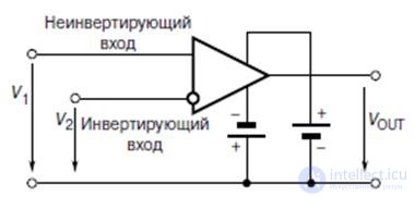
Fig.9.1. op amp circuit designation
OU has two inputs - inverting and non-inverting.
A non-inverting input is usually indicated by a ”+” sign or the letter ”p” (positive - positive), and an inverting input is indicated by a “-” sign, the letter “n” (negative - negative) and a circle. OU output voltage
V OUT = K V (V p -V n ),
where K V is the differential gain of the OS.
The difference between the input voltages V D = V p - V n is called the differential input voltage.
The sum of the input voltages V C = (V p + V n ) / 2 is called the common-mode input voltage.
To ensure that the operational amplifier can work with both positive and negative input signals, bipolar supply voltage should be used. For this you need to provide two sources of constant voltage, which, as shown in Fig.7.1, are connected to the corresponding external terminals of the OU. Most often, integrated operational amplifiers are designed for a supply voltage of ± 15 V, although there are quite a few models that are powered from sources of both substantially higher and much lower voltages. In the future, considering the schemes at the OS, we, as a rule, will not indicate power outlets.
An operational amplifier is almost always covered by a deep negative feedback , the properties of which determine the properties of the circuit with an opamp. The principle of introducing negative feedback is illustrated in Fig.7.2.
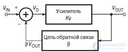
Fig.9.2. The principle of negative feedback
The output of the amplifier through the feedback circuit with the transfer coefficient _β (| β | ≤1) is connected to its input. OU output voltage
V OUT = K V V D = K V (V IN - βV OUT )
The gain of the circuit covered by the feedback
K = V OUT / V IN = K V / (1 + βK V )
The product of βK V is called the loop gain.
In practice, K V >> 1 (tens and hundreds of thousands), and the value of β lies within 0.01 ... 1. Then βK V >> 1 and the gain of the OU covered by the feedback) will be
K≈ 1 / β
From this relationship, it follows that the gain of a circuit with negative feedback is mainly determined by the properties of the external feedback circuit and is practically independent of the parameters of the amplifier itself. In the simplest case, the feedback circuit is a resistive voltage divider. In this case, the circuit with an op amp operates as a linear amplifier, the gain of which is determined only by the feedback coefficient. If RC_chain is used as a feedback circuit, an active filter is formed. Finally, the inclusion of diodes and transistors in the feedback circuit of an opamp allows one to realize nonlinear signal transformations with high accuracy.
To clarify the principles of operation of circuits at the OS and simplify their analysis, we will further use the concept of an ideal operational amplifier. The ideal op amp has the following properties:
a ) infinitely large differential voltage gain K V = ΔV OUT = / Δ (V p - V n ) (for real op amps K V lies within 10 3 ... 30 ・ 10 6 );
b ) zero zero offset voltage V OFF , i.e., if the input voltages are equal, the output voltage is zero regardless of the common-mode input voltage (for real OU V OFF , reduced to the input is within (1 μV ... 50 mV);
c ) zero input currents for both inputs (for real OU, they range from hundredths of pA to units of μA);
d ) zero output impedance (for real low-power op amps from tens of ohms to units of kΩ);
e ) the common-mode gain is zero;
f ) instantaneous response to a change in input signals (for real op-amps, the time to establish the output voltage ranges from units ns to hundreds of microseconds).
The operational amplifier intended for universal application, for reasons of stability, should have the same frequency response as the first-order low-pass filter (inertial link), and this requirement must be satisfied at least up to the unit gain frequency f T , t. e. frequency
at which | K V | = 1. In Fig.7.2, a typical logarithmic amplitude-frequency characteristic (LAFC) of the corrected operational amplifier is presented.
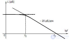
Fig.9.2. Typical LAFC operational amplifier
In a complex form, the differential gain of such an amplifier is expressed by the formula:
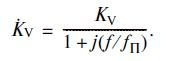
where K V - differential gain OU DC, frequency f P , corresponds to the border of the passband at the level of 3 dB. In the frequency range from f P to f T , the gain modulus is inversely proportional to the frequency, which leads to the simple relation
K V f P = f T
In other words, the frequency of the unit gain f T is equal to the product of the gain by the bandwidth. It should be borne in mind that this statement is valid only for amplifiers with complete internal correction.
Figure 9.3 shows the scheme of differential connection of an OS. \
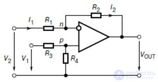
Fig.7.3. Differential inclusion OU
The output voltage of the amplifier with this inclusion
When the ratio of R 1 R 4 = R 2 R 3
V OUT = (V 1 -V 2 ) R 2 / R 1
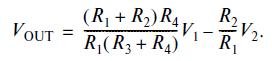
In the case of an inverting switch-on (Fig.9.4), the non-inverting input of an op-amp connects to the common bus.
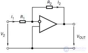
Fig.9.4. OA Inverting
The output voltage of the amplifier in the inverting switch is in antiphase with respect to the input. For this circuit, the input voltage gain, depending on the ratio of the resistors, can be either greater than one or less than one.
K = V OUT / V 2 = R 2 / R 1
The input resistance of the circuit is R IN = R 1 .
With a non-inverting switch-on, the input signal is fed to the non-inverting input of an op-amp, and the signal from the amplifier output (Fig.9.5) is fed to the inverting input through a divider on resistors R 1 and R 2 .
Fig.9.5. OS non-inverting
Circuit gain
K = V OUT / V 1 = 1 + R 2 / R 1
When a non-inverting op-amp is turned on, the output signal is in phase with the input signal and the voltage gain cannot be less than one. In the limiting case, if the output of an op-amp is short-circuited with an inverting input, this coefficient is equal to one. Such schemes are called non-inverting repeaters and are manufactured serially as separate ICs by several amplifiers in a single package. The input impedance of this circuit is ideally infinite. The repeater on a real operational amplifier has this resistance of course, although it is very large.
For a proportional change of the signal, or scaling, or, which is the same, multiplying by a constant factor, OA can be applied both in inverting (Fig. 7.4) and in non-inverting switching on (Fig. 7.5). Inverting inclusion is preferable for the following reasons:
- simple implementation of the transfer ratios both greater and less than one,
- no common mode signal,
- it is easy to ensure protection of the inputs of the OS with overload
- the scaling operation can be combined with the summation operation.
For the summation of several voltages can be applied OV in inverting inclusion. Input voltages through additional resistors are fed to the inverting input of the amplifier (Fig.9.6).
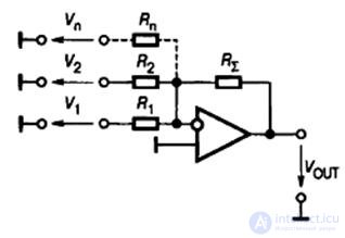
Fig.9.6. Inverting adder circuit
Output voltage of the circuit:
V OUT / R Σ = - (V 1 / R 1 + V 2 / R 2 +… + V n / R n )
It should be borne in mind that in multi-input adders, the bandwidth of the circuit is narrowed due to a decrease in loop gain due to the parallel connection of the input resistances of the channels. In this case, the scaling factors (transmission) for all inputs are set independently of each other. Thus, in the case of equal-scale summation of n input signals in an adder circuit at a fully adjusted opamp, the passband will narrow n times compared to a conventional single-input inverter with the same transmission coefficient.
To implement the operations of integration, an inverting inclusion of an OS is used (Fig.9.7).
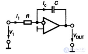
Fig.9.7. Inverting Integrator Diagram
The output voltage of the circuit is determined by the expression:
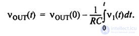
The constant term V OUT (t) defines the initial integration condition. Using the wiring diagram shown in Fig.9.8. You can implement the necessary initial conditions.
Fig.9.8. Integrator with a chain of initial conditions
When the key S 1 is closed and S 2 is open, this circuit works in the same way as the circuit shown in Fig.9.7. If the key S 1 is opened, the charging current with an ideal op-amp will be equal to zero, and the output voltage will retain the value corresponding to the moment of switching on. To set the initial conditions when the key S 1 is open, close the key S 2 . In this mode, the circuit simulates a first-order inertial link and after the end of the transient process, the duration of which is determined by the time constant R 3 C, a voltage will be established at the integrator output
V OUT = - (R 3 / R 2 ) V 2 (9.1)
After the key S 1 is closed and the key S is opened, the integrator begins to integrate the voltage V 1 , starting from the value (9.1).
Such integrators are manufactured by industry. For example, Burr-Broun manufactures an ASF2101 dual-channel integrator chip containing two op amps with input currents
0.1 pA, reset and storage keys and two 100 pF integrating capacitors.
Swapping the resistor and condensates in the integrator circuit
(Fig.9.8) we get a differentiator (Fig.9.9).
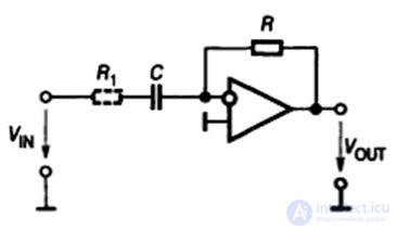
Fig.9.9. Differentiator circuit
The output voltage of this circuit
V OUT = - RC (dV IN / dt)
The practical implementation of the differentiating scheme shown in Figure 9.9 presents considerable difficulties for the following reasons:
- the circuit has a pure capacitive input resistance, since one of the terminals of the input capacitor is tied to the virtual ground. In the event that the input source is a different op amp, this may cause its instability,
- differentiation in the high-frequency region leads to a significant increase in the high-frequency components, which, as a rule, worsens the signal-to-noise ratio,
- in the feedback loop of an op-amp, the first-order inertial link is turned on, creating a phase delay of up to 90 ° in the high-frequency region, it is summed up with an op-amp phase delay, which can be or even exceed 90 °, as a result of which the circuit becomes unstable.
Eliminating these shortcomings allows the inclusion in series with the capacitor of an additional resistor R 1 (shown in Fig.9.9 by a dotted line). It should be noted that the introduction of such a correction practically does not reduce the range of operating frequencies of the differentiation scheme, since at high frequencies it still does not work satisfactorily due to a decrease in the gain of the control amplifier.
For accurate measurements of weak currents in a number of devices, a voltage proportional to the current is required. In many cases, it is necessary that the voltage source controlled by the current, also called the current-voltage converter, have as little as possible the input and output resistances. The circuit of the voltage source controlled by the current is shown in Figure 9.10.
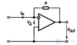
Fig.9.10. Current-controlled voltage source
If the amplifier is perfect, then V D = 0 and V OUT = - RI IN . If the gain of the op amp K V is finite, then the input and output impedance of the circuit:
R IN = V V / I IN = R / (1 + K V ) ≈ R / K V ,
R OUT = r OUT (R + R S ) / (R S K V ),
where r s is the impedance of the input source.
Voltage-controlled current sources (voltage-to-current converters) are designed to provide load current that is independent of the output voltage of the op-amp and is regulated only by the input voltage of the circuit. Such sources are used in measuring circuits, for example, when measuring resistance, in an electric drive, if it is required to stabilize the torque of an electric motor, etc.
The ideal voltage-to-current converter has infinitely large input and output impedances.
The current source circuit with grounded load is shown in Fig.9.11.
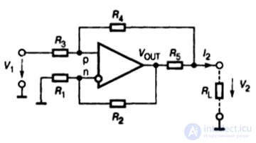
Fig.9.11. Voltage controlled current source for grounded load
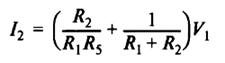
If you choose R 1 = R 3 and R 2 = R 4 , then the expression for the output current of the source will be:
In a variety of applications, the problem of separating signals and noise from a mixture that occupies a wide band of frequencies and components that occupy a narrower band is often solved. Devices that perform this task are called filters. Filter properties are usually described by transfer functions that are equal to the ratio of Laplace images of the output and input filter signals. For example, the transfer function of a low-pass filter (low pass filter, passes low frequencies and suppresses high frequencies) in general can be written as
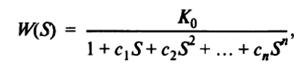
where с 1 , с 2 , ..., с n - positive real coefficients, К 0 - filter gain at zero frequency. The order of the filter is determined by the maximum degree of the variable S.
A filter with a given transfer function can be implemented on different components, in particular, with the help of circuits with capacitors and inductors. However, in some cases, it is inconvenient to deal with inductances because of their large size and complexity of their manufacture. Circuits with operational amplifiers allow the transfer functions to be implemented without the use of inductors. Filter circuits built on an OS are called active filters. The theory of calculations of active filters is well developed, there are relevant guidelines and programs for calculation. In this section, we will consider, for example, the simplest second-order low-pass filter (Fig.9.12).
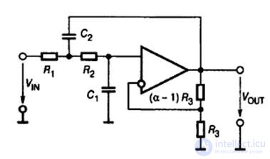
Fig.9.12 Active second-order low-pass filter
Negative feedback generated by the voltage divider R 3 , (α - 1) R 3 , provides a gain factor equal to α. Positive feedback due to the presence of a capacitor C 2 . The transfer function of the filter is:
Calculation of the filter consists in determining the values of resistors and capacitors included in the circuit.
Active filters are available in the form of integrated circuits by many companies, for example, AF100 / 150 (National Semiconductor), LTC1562 (Linear Technology), MAX270 / 271 or MAX274 / 275 (Maxim). They have a tunable cut-off frequency of up to several hundred kilohertz, order up to the eighth, and often a programmable type of filter.
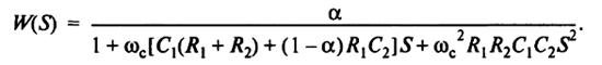
In some applications, it is necessary to form a voltage V 2 that would be a non-linear function of voltage V 1 , that is, V 2 = f (V 1 ), for example, V 2 = V a log (V 1 / V b ). Для реализации таких зависимостей применяют либо физические эффекты, которые позволяют реализовывать заданные зависимости, либо аппроксимируют их полиномиальными или степенными рядами.
В частности, в логарифмирующих и экспоненциальных преобразователях для получения требуемой функциональной характеристики используются свойства pn перехода диода или биполярного транзистора, смещённого в прямом направлении. На рис.9.13 приведена схнма логарифмического преобразователя.
Рис.9.13. Схема логарифмического преобразователя
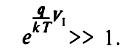
Ток диода приближённо описывается выражением:
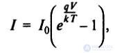
где V – напряжение на диоде, q – заряд электрона, k – постоянная Больцмана, I 0 – обратный ток диода, T – температура в градусах Кельвина.
When the condition V 1 / R 1 >> I 0 is met, the voltage at the output of this circuit
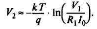
Fig.9.14 shows the scheme of the exponential converter.
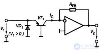
Fig.9.14. Exponential converter circuit
The output voltage of this circuit is determined by the expression:
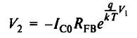 ,
,
at
Генераторы сигналов являются неотъемлемым элементом значительной части электронных устройств. Это могут быть как генераторы синусоидальной формы, так и генераторы сигналов специальной формы для различного рода измерительных и индикаторных устройств. В зависимости от конкретного применения к генераторам предъявляются самые разнообразные требования. Так для генераторов синусоидальных сигналов – это точность, монохромность и стабильность заданной частоты, для импульсных генераторов – это точность и стабильность заданного периода повторения и длительности импульсов, для генераторов сигналов специальной формы – это стабильность и точность воспроизведения заданного вида колебания. Во многих случаях в генераторах должна быть предусмотрена возможность внешнего управления параметрами выходного сигнала ( частотой, фазой, временными параметрами и формой колебаний). Схемотехнически электронный генератор представляет собой усилитель, охваченный положительной обратной связью. Усилители могут быть построены на дискретных транзисторах, на базе цифровых микросхем или операционных усилителей. Использование ОУ позволяет построить стабильные генераторы с весьма точным воспроизведением заданной формы выходного сигнала.
В качестве примера генераторов на ОУ рассмотрим релаксационные генераторы.
Релаксационными называют генераторы, у которых усилитель работает в переключательном режиме. К ним относятся автоколебательный и ждущий мультивибраторы, генераторы пилообразных и треугольных колебаний. Основой релаксационных генераторов на ОУ является обычно регенеративный компаратор, называемый также триггером Шмидта. Регенеративный компаратор может быть выполнен на ОУ с резистивной положительной обратной связью (рис.9.15).
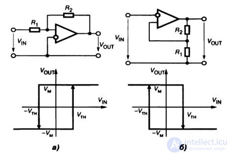
Рис.9.15. Триггер Шмидта, а) неинвертирующий б) инвертирующий
Переходная характеристика компаратора имеет гистерезис, ширина которого равна удвоенному пороговому напряжению 2V TH , причём, для схемы на рис.9.15а
V TH = V M R 1 /R 2 ,
а для схемы на рис 9.15б
V TH = V M R 1 /(R 1 + R 2 ),
где V M – максимальное выходное напряжение усилителя ( напряжение ограничения или насыщения).
На рис.9.16 приведена схема и временная диаграмма работы автоколебательного мультивибратора, построенного на базе триггера Шмидта.
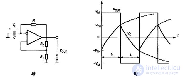
Рис.9.16. Автоколебательный мультивибратор: а) схема, б) временная диаграмма работы
Мультивибратор состоит из инвертирующего триггера Шмидта, охваченного отрицательной обратной связью с помощью интегрирующей RC-цепочки. Когда напряжение на конденсаторе V C достигает одного из порогов срабатывания, схема переключается и её выходное напряжение скачком принимает противоположное значение. При этом конденсатор начинает перезаряжаться в противоположном направлении, пока его напряжение не достигнет другого порога срабатывания. В этот момент схема переключится в первоначальное состояние.
Период колебаний мультивибратора равен
T = 2t 1 = 2RC ln( 1 + ( 2R 1 /R 2 ))
Для того, чтобы перейти от схемы автоколебательного к схеме ждущего мультивибратора, необходимо ввести дополнительно цепь запуска и цепь торможения. Назначение ждущего мультивибратора – получение одиночного импульса заданной длительности, начинающегося от фронта специального запускающего импульса. Схема одновибратора и временная диаграмма работы приведены на рис.9.17.
Длительность импульса ждущего мультивибратора (одновибратора):
t И = RC ln( 1 + ( R 1 /R 2 )·(1 + ( V Д /V М ))),
где V Д – падение напряжения на открытом диоде VD 1 .
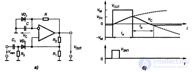
Рис.9.17. Ждущий мультивибратор : а) схема, б) диаграмма работы
Длительность импульса ждущего мультивибратора (одновибратора):
t И = RC ln( 1 + ( R 1 /R 2 )·(1 + ( V Д /V М ))),
где V Д – падение напряжения на открытом диоде VD 1 .
1.Нарисуйте схемное обозначение операционного усилителя и приведите формулу для выходного сигнала.
2.Принцип отрицательной обратной связи и выражение для выходного сигнала и коэффициента усиления операционного усилителя, охваченного отрицательной обратной связью.
3. Дифференциальное включение ОУ.
4. Инвертирующее включение ОУ.
5. Неинвертирующее включение ОУ.
6. Схема инвертирующего сумматора на ОУ.
7. Схема инвертирующего интегратора на ОУ.
8. Схема дифференциатора на ОУ.
9. Источник напряжения, управляемый током, на ОУ.
10. Источник тока, управляемый напряжением, для заземлённой нагрузки, на ОУ.
11. Активный ФНЧ второго порядка на ОУ.
12. Схема логарифмического и экспоненциального преобразователей на ОУ.
13. Триггер Шмидта на ОУ.
14. Автоколебательный мультивибратор на ОУ.
15. Схема ждущего мультивибратора на ОУ.

Comments
To leave a comment
Computer circuitry and computer architecture
Terms: Computer circuitry and computer architecture