Lecture
A wide range of ready-to-use, high-performance power supplies are available for powering electronic circuits, allowing you to select the optimal solution.
Among the variety of power converters, the following notation was established:
- DC / DC - converter converts direct current into direct current in order to obtain a different voltage, increased stability and / or galvanic isolation of one voltage from another,
- AC / DC - power supply, has an input current at the input, at the output - a direct current with the necessary parameters,
- DC / AC - inverter, converts direct current into alternating current, is used, for example, in backup power sources, where it converts direct voltage from batteries into alternating current for powering electrical appliances.
An ideal power source should provide the required values of supply voltages in the face of changes over a wide range.
environmental parameters, load values and input voltage. At the same time, it must have 100% efficiency. Real sources have the instability of the output voltage and interfering ripple.
The standard scheme of building a stable power source involves the use of negative feedback to compensate for the influence of destabilizing factors. In this case, the output voltage of the source is compared with some constant reference (reference) voltage. Such stabilized power sources belong to the class of compensatory. The regulating element of voltage stabilizers is a bipolar or field effect transistor. If this transistor works all the time in the active mode, then the circuit is called a linear (continuous) voltage stabilizer (LSN), and if the regulating transistor operates in the key mode, it is a pulsed (SPI). According to the stabilizers used, the power sources are called linear and pulsed.
Table 12.1 shows typical comparative characteristics of linear and switching power supplies. Stability in voltage and current is usually better for linear power supplies, and efficiency is better for pulsed ones. Therefore, in pulsed power supplies, additional linear stabilizers are often used to improve the output voltage parameters.
Table 12.1. Comparison of switching and linear power supplies
| Parameter | Linear | Pulsed |
| Input voltage instability,% | 0.02 - 0.05 | 0.05 - 0.1 |
| Load current instability,% | 0.02 - 0.1 | 0.1 - 1.0 |
| Output pulsations, mV | 0.5 - 2 | 25 - 100 |
| Efficiency,% | 40 - 55 | 60 - 95 |
| Average power density, W / dm 3 | ||
| Recovery time, ms | ||
| Retention time, ms |
In addition, it should be noted that switching power supplies have a wider range of permissible input voltages. For linear it usually does not exceed 10% of the nominal value and is directly related to efficiency (efficiency). For pulsed sources, the change in the input voltage affects the efficiency slightly, which allows you to work with strong changes in the mains voltage (up to 40%).
Linear voltage regulators include power regulators and a more or less complex low-power control circuit.
The principal difficulty in creating integral stabilizers lies in the fact that power transistors dissipate considerable power, causing local heating of the crystal. This dramatically affects the stability of the parameters of the control circuit, which includes the reference voltage source, differential error amplifier, protection circuit against overcurrent and short circuit load, overheating of the crystal and other emergency or abnormal conditions.
In simplified form, the linear voltage regulator circuit is shown in Figure 12.1. The circuit consists of an operational amplifier in a non-inverting turn-on with negative voltage feedback, a reference voltage source V REF and a control transistor VT 1 connected in series with the load.
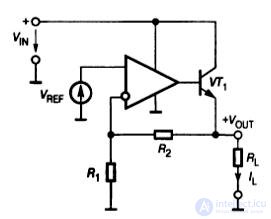
Fig.12.1. The basic scheme of linear voltage regulator
The output voltage V OUT is controlled by a negative feedback circuit, made on the resistive divider R 1 R 2 . The OS plays the role of an error amplifier, which is the difference between the reference voltage V REF , given by the reference voltage source (ION), and the output voltage of the divider R 1 R 2 .
ΔV = V REF - V OUT (R 1 / (R 1 + R 2 ))
The scheme works as follows. Let for one reason or another (for example, due to a decrease in the load resistance or an input unregulated voltage) the output voltage of the stabilizer V OUT decreased. At the same time, an error ΔV> 0 appeared at the input of the OU. The output voltage of the amplifier will increase, which will lead to an increase in the base current and, consequently, the current emitter of the control transistor to a value at which the output voltage will increase almost to the original level.
In the case of an ideal op amp, the steady-state error value that coincides with the differential input voltage of the op-amp is close to zero. It follows that
V OUT = V REF (1 + R 2 / R 1 )
The power of the operational amplifier is provided from the input unregulated unipolar voltage, in this case positive. This imposes restrictions on the allowable range of input and output signals, which in these conditions should only be positive. However, for power supply circuits such a limitation does not play a role, therefore, the use of voltage of the other polarity to power the OU can be waived. Although the operational amplifier is powered by an unstabilized input voltage V IN , due to the deep negative feedback, the influence of this factor on the stability of the output voltage is small.
The described scheme is intended mainly for stabilization of positive voltages relative to the common point of the circuit. To stabilize negative voltages, the same circuit can be used, if one uses an input voltage galvanically isolated from a common point. In this case, the output of the stabilizer is connected to a common point, and the minus output of the circuit is the connection point of the negative terminal of the input voltage source and the common point of the stabilizer.
For cases when two stabilized voltages symmetrical with respect to a common point (for example, ± 15 V for powering operational amplifiers) are required, integrated circuits are produced that contain two stabilizers for positive and negative voltages, for example, NE5554. A simplified diagram of the internal structure of such a stabilizer is shown in Figure 12.2a, and a typical scheme for its inclusion is shown in Figure 12.2b.
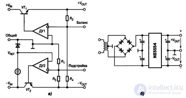
Fig.12.2. Stabilizer of two monopolar voltages: a) schematic diagram, b) typical switching circuit
In circuits powered by batteries and rechargeable batteries, it is desirable to have a minimum voltage drop across the stabilizer. When using bipolar transistors as regulating elements, the minimum voltage drop required for normal operation is about 3 V.
A significant reduction in the minimum allowable voltage drop at the stabilizer can be achieved by using a MOSFET connected as a power source as a power regulator. A simplified diagram of such a stabilizer is shown in Figure 12.3. A p-channel transistor operating in the enrichment mode is used to stabilize the positive voltages.
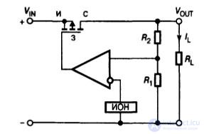
Fig.12.3. Voltage stabilizer with a regulating MOSFET
The scheme works as follows. When the load resistance decreases, the output voltage also decreases, and an error ΔV <0 will appear at the amplifier output. The output voltage of the amplifier will decrease, reducing the voltage at the gate of the regulating MOS transistor. Since this is a p-channel transistor, a decrease in the voltage at its gate will cause an increase in the drain current and the output voltage will increase to the same value.
A big advantage of stabilizers with a regulating MOS transistor is the independence of the current consumption (common output current) from the load current. This is due to the fact that the MOSFET is controlled by the voltage, and its gate current (and hence the output current of the sensor) is completely insignificant compared to the load current.
Another advantage is that the voltage drop across the regulating element can be reduced to very small values unattainable for bipolar transistors. For example, the MAX8865 dual-channel voltage regulator has a minimum allowable voltage drop of 55 mV at a load current of 50 mA and only 1 mV at a load current of 1 mA.
Next, we consider possible switching circuits for linear stabilizers on the example of a three-output voltage regulator KR142EN5A. It is designed for a fixed voltage of 5 V, the permissible output current of 1A, there is an internal thermal protection, protection of the output transistor and an internal short circuit current limiting.
Figure 12.4 shows a typical wiring diagram. C 1 and C 2 capacitors are included for increased stability.
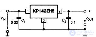
Fig.12.4. Typical wiring diagram
If it is necessary to increase the fixed value of stabilization, you can turn on the Zener diode's common output circuit of the stabilizer and increase the stabilization voltage by the value of V CF (Figure 12.5).
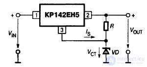
Fig.12.5. Increase in fixed voltage stabilization
It is possible to increase the stabilization voltage and make it adjustable if the common output is energized from the divider through a non-inverting repeater to the OU (Figure 12.6).
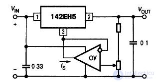
Fig.12.6. Stabilizer with adjustable output voltage
It is possible to increase the maximum output current of the stabilizer by turning on an additional powerful transistor, as shown in Figure 12.7.

Fig.12.7. Schemes to increase the maximum output current with the inclusion of an additional high-power transistor: a) with a common emitter, b) with a common collector
The disadvantage of such a circuit is that the built-in current limiting and protection circuit of the output transistor of the stabilizer itself do not depend on the load current and are not actually used for their intended purpose. But due to a slight complication, it is possible to provide protection against a short circuit at the output (Fig. 12.8).
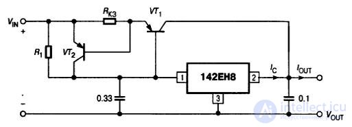
Fig.12.8. Stabilizer with high output current and short circuit protection
A diagram of a stable current source based on a voltage regulator is shown in Figure 12.9.
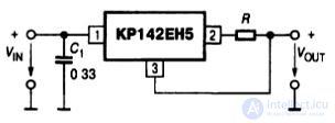
Fig.12.9. Stable current source circuit
The resistance of the resistor R is determined by the expression
R = (V OUT NOM / I OUT )
On the resistor R, the voltage drops equal to the nominal output voltage of the stabilizer. Therefore, in such a scheme, it is desirable to use a stabilizer designed for a small voltage stabilization.
In the absence of a ready-made bipolar stabilizer, it can be constructed on the basis of a unipolar one (Figure 12.10).
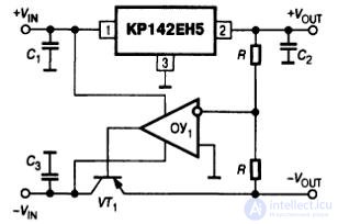
Fig.12.10. Bipolar stabilizer circuit
Since the potential of the non-inverting input of the op-amp 1 is zero, then the potential of the inverting input of this amplifier must be equal to zero. When the OS operates in the linear mode and the resistances of the resistors are equal in the divider, this can be only in the case of equality in absolute value of the bipolar voltages at the output of the circuit.
The principle of operation of continuous (linear) voltage regulators with a sequential regulating element is that when the input voltage and / or load current changes, the output voltage of the stabilizer (voltage at the load) is kept constant by changing the voltage drop across the regulating element. The difference between the input and output voltages falls on a powerful regulating transistor and, depending on the switching circuit and the range of variation of the input voltage, can reach several volts. As a result, a rather large power is dissipated when the load current flows through this transistor. This predetermines the relatively low efficiency of the linear stabilizer, which in the case of low stabilization voltages can fall below 50%.
Significantly large values of efficiency can be achieved if, instead of a continuous regulating element between the input voltage and the load, turn on a pulse switch (switch), which cyclically
(with a certain repetition period T) switches from the open (closed) state to the closed (open) state and back. In this case, the average value of the output voltage on the load will be determined by the ratio of the duration t OPEN of its open state to the repetition period. Thus, by changing the relative duration of the open state of the key, it is possible to regulate the average voltage on the load over a wide range. If an appropriate low-pass filter is turned on between the switch and our load, you can smooth out the voltage ripple on the load to the desired value.
With a small key resistance in the open state (ideally, it can be close to zero), the power loss on such a regulating element is very small, and in practice, the efficiency can reach 95% or more.
Power supplies with switches are called pulsed power sources, and if they stabilize the output voltage, then pulsed voltage stabilizers. Compared with continuous voltage stabilizers, pulsed sources have not only significantly higher efficiency, but also allow to obtain:
- the output voltage is greater than the input,
- output voltage of reverse polarity according to the input,
- stabilization of the output voltage with a wide (more than 50%) range of input variation,
- with an output power of tens or more watts - significantly smaller mass and dimensions.
The disadvantages of impulse sources are:
- the pulsed nature of voltages and currents in the circuit, which causes intense interference in the load, in the primary power source and in the surrounding space and requires the use of complex smoothing filters, careful shielding and detailed design of the structure,
- certain difficulties with ensuring the stability of pulsed devices with feedback,
- relatively long (compared with continuous devices) duration of transients.
The classification of switching power supplies is shown in Figure 12.11.
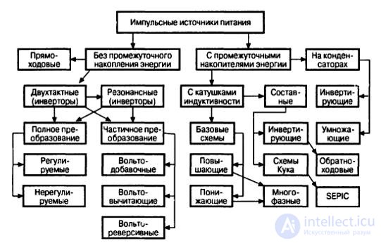
Fig.12.11. Classification of switching power supplies
Pulsed power sources are distinguished by a large variety of design principles and circuit solutions. They are divided into two large groups: with intermediate accumulation of energy and without intermediate accumulation of energy.
For pulsed power sources with intermediate accumulators, work in two cycles is typical, in one of which there is an accumulation of energy in an inductive coil (choke) or a capacitor, and in the second - the transfer of energy to the load. It is not possible to manufacture an inductive coil or a capacitor of relatively large capacity using the methods of integrated technology, therefore all pulsed integrated power supplies have external components.
Figure 12.12 shows a step-down pulse voltage stabilizer (PSI). The transistor switches from fully open to fully closed with a frequency of tens, hundreds of kilohertz, or even a few megahertz. When the transistor is open, the current from the primary energy source through the choke enters the load. In this case, the current I L grows and, as a result, energy accumulates in the inductor. When the transistor is closed, the current I L flows through the diode VD, continuing to feed the load. At the same time, the coil current decreases and the energy accumulated in the choke in the previous cycle is spent on maintaining the voltage across the V OUT load. The ratio of open and closed states of the key determines the magnitude of the voltage V OUT .
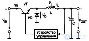
Fig.12.12. Scheme of lowering ISN
Figure 12.13 presents the block diagram of the control unit voltage regulator.
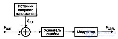
Fig.12.13. Control block diagram
The control unit compares the output voltage with the reference. If the output voltage decreases in comparison with the reference voltage, then the modulator of the control device increases the ratio of the open time of the transistor t OPEN to the period of the stabilizer pulse T, called the relative pulse duration
γ = t OPEN / T.
При увеличении ( уменьшении V OUT ) от номинального значения модулятор уменьшает ( увеличивает) значение γ. В отечественной литературе этот параметр называют также коэффициентом заполнения, а в английском обозначают термином duti cycle ( относительный рабочий интервал).
Принцип действия модулятора определяется законом модуляции. В импульсных стабилизаторах наиболее часто применяют широтно-импульсную или частотно-импульсную модуляции. Если регулируется время открытого состояния, то есть ширина импульсов, при постоянной частоте следования импульсов f = 1/T, то имеет место широтно-импульсная модуляция (ШИМ). Если относительная длительность импульса γ регулируется путём изменения частоты следования импульсов при их неизменной длительности, то такая модуляция называется частотно-импульсной модуляцией (ЧИМ).
В схеме на рис.12.12 выходное напряжение всегда ниже входного. Изменив расположение элементов в схеме, можно, используя свойство самоиндукции, получить выходное напряжение большее, чем входное (рис.12.14).
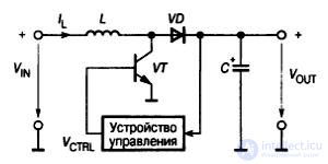
Рис.12.14. Схема повышающего ИСН
Когда транзистор VT открыт, к дросселю L приложено входное напряжение V IN . В этом случае согласно закону электромагнитной индукции
V IN = L(dI L /dt) ,
и ток в дросселе будет расти, увеличивая запасаемую в нём энергию. К диоду VD будет приложено запирающее напряжение, и ток нагрузки будет поддерживаться за счёт разряда конденсатора С. После запирания транзистора потенциал на его коллекторе поднимается до величины, превышающей выходное напряжение, за счёт ЭДС самоиндукции дросселя. Диод откроется. Ток в дросселе при этом будет убывать, и его энергия, запасённая в первом такте, вместе с энергией, поступающей от первичного источника, будет питать нагрузку и заряжать конденсатор.
Регулировочная характеристика повышающего преобразователя ( при условии, что ток дросселя нигде не достигает нуля) описывается следующим соотношением
 .
.
Примером интегральной микросхемы повышающего импульсного стабилизатора может служить микросхема MAX856 фирмы Maxim, преобразующая постоянное нестабилизированное напряжение от 0,8 до 6 В в постоянное напряжение 5 В при токе нагрузки до 100 мА. Кристалл, размером 2,1 х 1,5 мм в восмивыводном корпусе содержит устройство управления и коммутирующий МОП-транзистор. Диод, дроссель и конденсатор – внешние. КПД устройства при токе нагрузки в 40 мА достигает 85%. Ток, потребляемый самой микросхемой , составляет не более 25 мкА. Способ регулирования – ЧИМ, при частоте до 500 кГц. Устройство управления ограничивает входной ток величиной 0,5 А и контролирует напряжение первичного источника тока.
Схемы понижающего и повышающего преобразователей ( рис.12.12 и 12.14) являются базовыми для построения более сложных схем преобразователей. Простейшая составная схема, представляющая собой комбинацию этих двух преобразователей, представлена на рис.12.15.
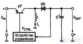
Рис.12.15. Схема инвертирующего ИСН
В этой схеме регулирующий транзистор включён последовательно с первичным источником, как в схеме понижающего преобразователя, а диод, через который протекает ток при запертом транзисторе, - последовательно с нагрузкой, как у повышающего преобразователя. Когда транзистор VT открыт, диод VD закрыт, и к дросселю приложено входное напряжение V IN . В этом случае согласно закону электромагнитной индукции ток в дросселе будет расти, увеличивая запасённую в нём энергию. Нагрузка питается за счёт разряда конденсатора С. Во втором такте, после запирания транзистора,
ток продолжает течь через дроссель и через открывшийся диод заряжает конденсатор в направлении, противоположном полярности входного напряжения. Получающаяся при этом регулировочная характеристика

Таким образом, на выходе инвертирующего импульсного стабилизатора напряжение не только имеет полярность, обратную полярности входного напряжения, но в зависимости от относительной длительности импульса может быть как больше, так и меньше входного.
Примером инвертирующего стабилизатора может служить микросхема MAX764 фирмы Maxim, преобразующая постоянное нестабильное напряжение 3…16 В в постоянное напряжение -5 В при токе нагрузки до 250 мА. Кристалл, размером 3,7 х 2 мм в восьмивыводном корпусе содержит устройство управления и коммутирующий МОП-транзистор. Диод, дроссель и конденсатор – внешние. КПД устройства при токе нагрузки в 200 мА достигает 80%. Ток, потребляемый самой микросхемой, составляет не более 90 мкА. Способ регулирования - ЧИМ, при частоте импульсов до 300 кГц. Устройство управления ограничивает входной ток величиной 0,75 А.
Рассмотренные ранее преобразователи постоянного напряжения имеют ряд ограничений при практическом использовании. В частности, наличие в них гальванической связи между входом и выходом не позволяет применять такие преобразователи в тех случаях, когда требуется гальваническая развязка. Другим ограничением является то, что при заданном диапазоне изменения входного напряжения питания возможный диапазон изменения выходного напряжения имеет вполне определённые пределы. То есть, нецелесообразно пытаться получать с помощью рассмотренных ранее схем напряжения в сотни вольт из напряжений в единицы вольт, и наоборот. Эти недостатки можно устранить, если дополнить их неким устройством, играющим роль трансформатора постоянного напряжения (ТПН).
Идеальный ТПН должен обеспечивать передачу постоянного напряжения с постоянным коэффициентом трансформации, высокую степень изоляции между первичной и вторичной цепями и возможность построения системы преобразования энергии с несколькими входами или выходами.
На рис.12.16 представлена функциональная схема наиболее широко применяемого ТПН.
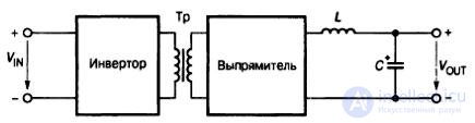
Рис.12.16. Функциональная схема ТПН
Функции отдельных звеньев ТПН вполне очевидны. Инвертор преобразует входное постоянное напряжение в переменное напряжение прямоугольной формы высокой частоты. Трансформатор Тр обеспечивает повышение или понижение переменного напряжения и гальваническую разделение первичной и вторияной цепей. Выпрямитель вновь преобразует переменное напряжение в постоянное.
Самым сложным узлом ТПН, во многом определяющим его свойства, является инвертор. Инверторами называются преобразователи постоянного тока в переменный. Семейство инверторов довольно обширно и включает устройства различного назначения, рассчитанные на передачу мощности от долей ватта до многих мегаватт.
Силовая часть инверторов может быть построена различным образом. На рис.12.17 приведены основные схемы силовых частей.

Рис.12.17. Основные схемы силовых частей инверторов: а) нулевая,
б) полумостовая, в) мостовая
Наименьшее количество элементов содержит нулевая схема, в которой один из выводов входного источника питания соединён с отводом от средней – нулевой – точки первичной обмотки трансформатора ( рис.12.17а). Ключи S 1 и S 2 поочерёдно замыкаются и размыкаются. При этом к соответствующим первичным полуобмоткам трансформатора прикладывается входное напряжение. Намагничивающие силы полуобмоток направлены в магнитопроводе в противоположные стороны, поэтому постоянное подмагничивание, в идеале, отсутствует. Трансформатор объединяет полуволны одного цикла коммутации и повышает или понижает их амплитуду в соответствии со своим коэффициентом трансформации. Недостатком этой схемы является повышенное напряжение на закрытом ключе. Поэтому такую схему применяют для преобразования относительно низких напряжений. Другой недостаток – менее эффективное, чем у двух других схем, использование трансформатора.
Полумостовая схема (рис.12.17б) широко применяется для построения сетевых источников питания небольшой мощности ( до сотен ватт). Входное напряжение делится пополам с помощью конденсаторов. Ключи также переключаются поочерёдно. При замыкании одного из ключей к первичной обмотке трансформатора прикладывается напряжение, равное V IN /2 , поэтому для передачи той же мощности, что и в предыдущей схеме, через ключи должен протекать вдвое больший ток. Напряжение на закрытых ключах не превышает входное напряжение.
Мостовая схема (рис.12.17в) применяется для источников мощностью от сотен ватт и выше. Ключи циклически меняют состояние : S 1 , S 4 – замкнуты, S 2 , S 3 – разомкнуты, и наоборот. К первичной обмотке трансформатора всегда прикладывается полное входное напряжение. Напряжение на закрытых ключах также не превышают входное напряжение.
Примером нерегулируемого нулевого инвертора может служить MAX845. Эта микросхема содержит задающий генератор, счётный триггер и два n-канальных МОП-транзистора (рис.12.18).
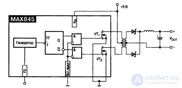
Рис.12.18. Схема включения интегрального нерегулируемого инвертора MAX845
Генератор в зависимости от состояния входа выбора частоты FS вырабатывает счётные импульсы частотой 400 или 700 кГц.
Счётный триггер TT делит эту частоту пополам и распределяет эти импульсы по затворам МОП-транзисторов. Допустимое напряжение сток-исток транзисторов всего 12 В, поэтому номинальное напряжение питания составляет 5В. Выходная мощность микросхемы не более 0,75 Вт. Ток собственного потребления не превышает 5 мА. Микросхема изготавливается в миниатюрных корпусах SO-8 и μMAX размером 3х5 мм.
Регулирование выходного напряжения инверторов, применяемых в схемах преобразователей постоянного напряжения, осуществляется, в основном, путём модуляции ширины выходных импульсов при постоянной частоте коммутации. В качестве примера регулируемого инвертора можно привести микросхему TL494 производства фирмы Texas Instruments. Функциональная схема TL494 приведена на рис.12.19, а типовая схема включения в качестве контроллера регулируемого двухтактного инвертора – на рис.12.20.
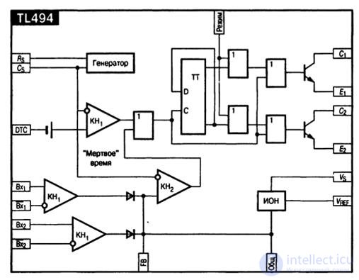
Рис.12.19. Функциональная схема TL494
Для стабилизации используются отрицательные обратные связи по напряжению и току.
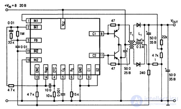
Рис.12.20. Типовая схема включения TL494
Для уменьшения размеров, веса и стоимости магнитных элементов и фильтровых конденсаторов необходимо повышать частоту переключения. Однако реальные потери в ключевых регулирующих элементах пренебрежимо малы лишь на относительно низких частотах переключения в пределах 20…40 кГц.
Потери на переключение вызваны тем, что переход от включённого состояния транзистора к выключенному и обратно происходит не мгновенно, а в течении определённого, пусть даже и малого времени. Во время переключения рабочая точка транзистора находится в активной области выходных характеристик (рис.12.21).
В идеале переключение транзистора следовало бы проводить по траектории 1. Например, для перевода транзистора из выключенного состояния (точка В) во включённое (точка А), следует сначала при нулевом токе уменьшить напряжение сток-исток V DS транзистора до нуля ( точка 0), а затем увеличить ток до установившегося значения. Практически же, если не приняты специальные меры, из-за наличия паразитных ёмкостей и индуктивностей переключение будет проходить по траектории 2. При этом на транзисторе выделяется значительная электрическая мощность, преобразующаяся в тепло.

Рис.12.21. Траектория переключения МОП-транзистора
Таким образом, для уменьшения потерь на переключение следует открывать транзистор, когда напряжение на нём равно нулю, а звкрывать при нулевом токе. Эти условия можно обеспечить за счёт использования резонансных колебаний в цепях с ключевыми элементами.
Упрощённая схема резонансного преобразователя, работающего при нулевом токе переключения ( так называемый ПНТ-преобразователь), показана на рис.12.22.
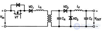
Рис.12.22. Схема резонансного переключателя, работающего при нулевом токе переключения
В этой схеме простой ключ заменён резонансным ключом, состоящим из компонентов VT, L R , C R . В принципе, в качестве резонансной индуктивности может использоваться индуктивность рассеяния трансформатора.
Пусть первоначально транзистор закрыт. Выходной ток течёт за счёт энергии, запасённой в дросселе выходного фильтра L F , через диод VD 3 в нагрузку. В некоторый момент времени, определяемый схемой управления, ключ VT открывается. Колебательный контур, образованный катушкой L R и конденсатором С R , начинает получать энергию. Заряд конденсатора C R и последующий его разряд будут происходить по закону, близкому к синусоидальному, с частотой, равной резонансной частоте контура L R C R . Одновременно ток в катушке L R также будет изменяться по синусоидальному закону – вначале увеличиваться, затем уменьшаться. Когда этот ток уменьшится до нуля, нужно закрыть ключ. При этом диод VD 1 предотвращает обратный ток через паразитный диод МОП-транзистора, который мог бы быть вызван продолжающимся резонансным процессом.
Когда ток в катушке L R становится равным нулю, выходной ток течёт через дроссель L F , диод VD 2 и конденсатор C R , который быстро разряжается.Как только он разрядится до нуля, открывается диод VD 3 . На этом один резонансный цикл заканчивается, и с открывания транзистора VT начинается следующий цикл. Так как транзистор открывается и закрывается при нулевом токе, потери на переключение будут минимальны. В связи стем, что переход тока с диода VD 2 к диоду VD 3 и обратно замедлен присутствием индуктивности L F и ёмкости C R , потери энергии будут снижены и в диодах. Уменьшаются также скорости нарастания токов и напряжений, что способствует снижению уровней электромагнитных помех и перенапряжений на элементах схемы.
В рассмотренной схеме переключение силового транзистора происходит при нулевом токе через него. Существуют также схемы, в которых транзистор переключается при нулевом напряжении (ПНН-преобразователи). Схемы ПНТ лучше подходят для сетевых источников питания с повышенным питающим напряжением; схемы ПНН – для преобразователей постоянного тока с более низким напряжением питания.
В общем случае можно сформулировать следующие достоинства и недостатки резонансных преобразователей по сравнению с обычными импульсными преобразователями на ту же мощность и работающими с той же частотой переключений.
Преимущества резонансных преобразователей:
- significantly lower switching losses, in particular, in the PNA mode, losses associated with the discharge of the output capacitance of the transistor through its open channel when unlocked;
- approximately fivefold reduction of electromagnetic interference;
- lower requirements for the elements, especially in relation to the maximum allowable rate of increase of voltages and currents;
- for the organization of resonant switching processes, parasitic reactivity of the circuit can be used.
Disadvantages of resonant converters:
- more complex power circuit;
- narrow range of regulation;
- in general, variable switching frequency;
- more complex control schemes.
1. Explain the designation DC / DC, AC / DC, DC / AC and explain the use of these devices.
2. Describe the main differences in the characteristics of the pulse and linear power sources.
3. The basic scheme of linear voltage regulator.
4. Schematic diagram of the stabilizer of two bipolar voltages and a typical scheme of its inclusion.
5. Voltage stabilizer with a regulating MOSFET.
6. A typical circuit for switching on a three-output voltage regulator KR142EN5A.
7. Increase the fixed voltage stabilization.
8. Stabilizer with adjustable output voltage.
9. Schemes to increase the maximum output current with the inclusion of an additional high-power transistor.
10. Stabilizer with high output current and short circuit protection.
11. Diagram of a stable current source.
12. Diagram of bipolar stabilizer.
13. The main advantages of pulse voltage regulators.
14. Scheme of lowering ISN.
15. Scheme of boosting ISN.
16. Scheme of the inverting SRI.
17. Functional diagram of the DC voltage transformer.
18. Main circuits of power units of inverters.
19. Diagram of a resonant switch operating at zero switching current.

Comments
To leave a comment
Computer circuitry and computer architecture
Terms: Computer circuitry and computer architecture