Lecture
FPGA (field programmable gate arrays) or FPGA (programmable logic integrated circuits) are digital integrated circuits (ICs) consisting of programmable logic blocks and programmable connections between these blocks.
Depending on the method of manufacturing the FPGA, they can be programmed either once or repeatedly. Devices that can only be programmed once are called once programmable.
The phrase "field programmable" contained in the FPGA abbreviation means that the programming of FPGA devices is done on-site, "in the field," unlike devices whose internal functionality is strictly prescribed by the manufacturer. Moreover, we can talk about the possibility of modifying the functions of the device embedded in the electronic circuit, which is already somehow used. If the device can be programmed, while remaining in the higher-level system, it is called internally programmable.
Currently, FPGAs fill four large market segments: custom integrated circuits, digital signal processing, embedded microcontroller-based systems, and microcircuits that provide the physical level of data transfer. In addition, with the advent of FPGA, a new market sector has emerged - systems with a tunable architecture, or reconfigurable computing (RC).
The main feature of the FPGA is their internal structure, which mainly consists of a large number of simple programmable logical blocks- “islands” into the “sea” of programmable internal links (Fig. 7.1).
In the fine-grained architecture, each logical block can be used to implement only a very simple function. For example, a block can be configured to operate as a 3-input simple logic element (AND, OR, NAND, and so on) or a memory element (D-type trigger, D-type latch, and so on).
Small-modular structures are used in the implementation of coherent logic and inhomogeneous structures like finite automata. Small-modular structures are also effective in the implementation of systolic algorithms (functions that are extremely efficient due to the implementation of mass parallelism). These structures have a certain advantage when using the technology of traditional logic synthesis, which is based on the fine-modular architecture of custom-made microcircuits.
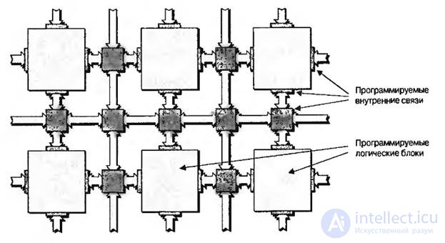
Fig.7.1. FPGA internal structure
For “fine-grained” FPGA, a large number of connections inside the blocks and between them are typical. As the modularity of devices increases to medium-modulus and higher, the number of connections in the blocks decreases. This is an important property, since internal communications determine the magnitude of the vast majority of delays associated with the passage of signals through the FPGA.
In the “middle modular” FPGA, each logical block contains a relatively large amount of logic compared to the “fine modular” FPGA. For example, a logical block can contain four 4-input matching tables, four multiplexers, four D-flip-flops, and a certain amount of fast transfer logic.
“Large-module” FPGAs contain arrays of nodes, where each node is a complex element that implements algorithmic functions, such as, for example, the fast Fourier transform or the core of a general-purpose microprocessor.
There are two main ways to implement programmable logic blocks used to form medium-modular devices: based on multiplexers (MUX - from multiplexer) and based on correspondence tables (LUT –from lookup table).
As an example of the implementation of devices based on multiplexers, consider the 3-input function y = (a & b) + c, implemented using a block containing only multiplexers (Fig.7.2).

Fig.7.2. Logic block on multiplexers
The device can be programmed in such a way that each of its inputs can be given a logical 0 or a logical 1, or a direct or foreign value of the input signal (in our case a, b or c) coming from another block or from the input of the microcircuit. This approach allows for each block to create a huge number of configuration options for performing various functions (x at the input of the central multiplexer in Fig. 7.2 indicates that any signal can be input - 0 or 1).
The basic concept of correspondence tables is simple. In such chips, a group of input signals is used as an index (pointer, or cell address) of the correspondence table. The contents of this table are organized in such a way that the cells indicated by each input combination contain the desired output value. For example, in Fig. 7.3, the circuit on logic elements and its truth table for the function y = (a & b) + c are shown.
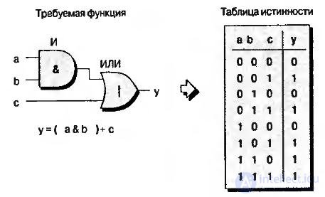
Fig.7.3. Required function and its truth table
To implement this function, you need to load the 3-input table with the appropriate values. Now let's assume that the correspondence table is formed from the memory cells of static RAM (it can also be formed by incremental jumpers, EEPROM or Flash memory cells). To select the required cell of RAM using a cascade of transfer valves, input signals are used, as shown in Fig. 7.4. At the same time, the memory cells of static RAM for loading configuration data should be connected in a long chain, but these chains are not shown in Fig. 7.4 in order to simplify it.
In the diagram, the open or active transfer valve passes the signal from input to output. A closed valve electrically disconnects its output from the conductor to which it is connected. The transfer valves, on the designations of which a small “circle” is shown, are activated when logical 0 is sent to the control input. Conversely, the valves, which do not have a circle, are activated when the level 1 logical input is applied to the control input. Based on this, it is easy to see how various input combinations can be used to select the contents of the desired memory cell.
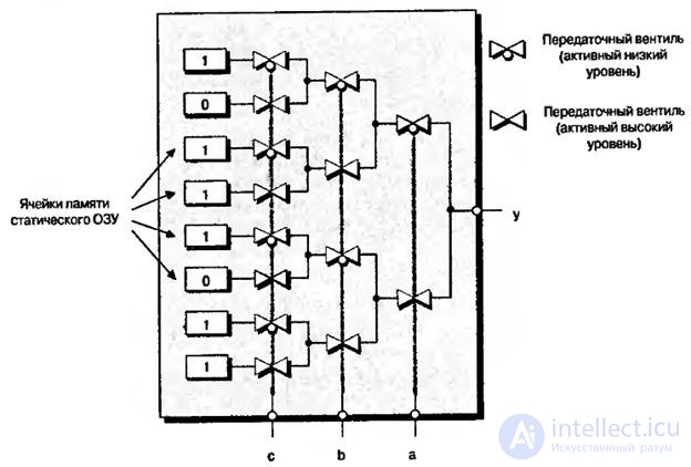
Fig.7.4. Correspondence table based on transfer valves
Multiplexer-based architectures, unlike blocks based on correspondence tables, do not support high-speed logical transfer chains. Therefore, most modern FPGA architectures are implemented on the basis of correspondence tables.
The core of the correspondence table in a static RAM device uses several memory cells for its operation. This allows you to use some interesting features. In addition to the main purpose, that is, the formation of a correspondence table, devices of some suppliers allow the use of cells that form the table as small blocks of RAM. For example, 16 memory cells that form a 4-input table can act as a 16 × 1 RAM block. Such memory areas are called distributed RAM, because, firstly, the correspondence tables are scattered (distributed) over the entire surface of the crystal, and secondly, this name distinguishes them from large RAM blocks.
Another alternative use of the tables is based on the fact that all configuration cells, including those that form the correspondence table, are effectively connected together in one long chain (Fig. 7.5).
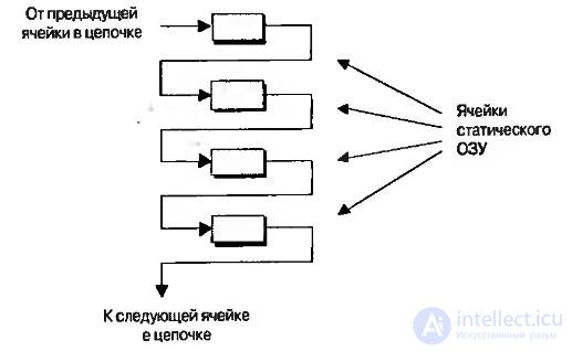
Fig.7.5. Chained configuration cells
The fact is that in some devices the memory cells that form the correspondence table can be considered independently of the main structure of the chain after programming and used as a shift register. Thus, each correspondence table can be considered as a multifunctional component (Fig.7.6).

Fig.7.6. Multifunctional table of compliance
Different manufacturers logical units can be called differently, which does not change their essence. In the FPGA company Xilinx blocks are called logical cells (logic cell). Among other things, the logic cell contains a 4-input matching table, which can work as RAM 16 • 1 or as a 16-bit shift register, as well as a multiplexer and a register (Fig. 7.5).
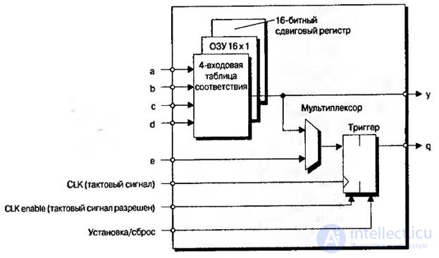
Fig.7.5. Simplified view of Xilinx logic cell
The polarity of the clock signal (trigger response to the front or the fall of the clock) can be set programmatically, as well as the polarity of the signals “clock signal enabled” and “set / reset” (active high or low).
In addition to the correspondence tables, multiplexers, and registers, logical cells contain a small number of other elements, including fast transfer logic for use in arithmetic operations.
The logical blocks that make up Altera FPGAs are called logical elements (logic element). There are a number of differences between the logical cells of Xilinx and the logical elements of Altera, but in general their concepts are very similar.
The next step in the hierarchy of the construction of microcircuits of programmable logic is, so-called, by definition, the company Xilinx, section (slice). Fig.7.6 shows a section of two logical cells.

Fig.7.6. Section containing two logical cells
In Fig.7.6 for simplicity, internal communications are not shown, it should also be noted that although the correspondence tables, multiplexers and registers of each cell have their own data inputs and outputs, the section has common clock signals, clock resolutions and set / reset for both logic cells.
Climbing up the hierarchy, we reach a level that Xilinx calls a configurable logic block CLB (CLB). The company Altera, in turn, calls it a block of logical arrays or LAB (logic array block). Other FPGA vendors give them their equivalent names.
Configurable logic blocks inside the FPGA can be represented as “islands” of programmable logic in the “sea” of programmable connections (Fig.7.7).
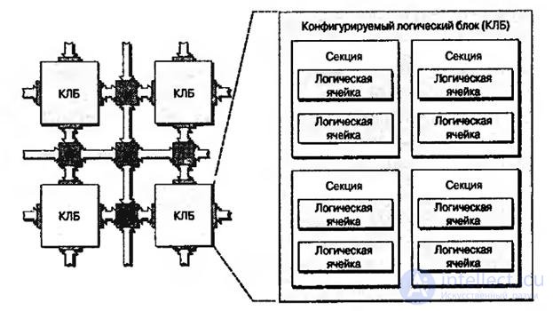
Fig.7.7. Part of the internal structure of the FPGA containing four LPR, each of which contains four sections
Inside the CLB, there are fast, programmable internal connections that are used to communicate between adjacent sections.
The reason for the existence of such a logical-block hierarchy, that is, a logical cell → a section with several cells → a configurable logic unit with several sections, is that it is supplemented with an equivalent hierarchy of internal connections. In other words, there are fast internal connections between logical cells within a section, then less fast connections between sections in a configurable logic block (CLB) and a connection between CLBs. Such a hierarchy reflects the step-by-step achievement of an optimal compromise between the ease of interconnecting internal structures and excessive signal delays on internal interconnections.
As already noted, each 4-input matching table can be used as a 16 × 1 RAM block. In the four-section LLB shown in Fig.7.7, all correspondence tables inside this block can be configured to implement the following functions:
· Single-port RAM block 16 • 8 bits.
· Single-port block of RAM 32 • 4 bits.
· Single-port RAM block 64 • 2 bits.
· Single-port RAM block 128 • 1 bit.
· Dual port RAM block 16 • 4 bits.
· Two-port block of RAM 32 • 2 bits.
· Dual port RAM block 64 • 1 bit.
A port is usually referred to as a set of control signals and data that are considered as a unit. In single-port RAM, data is written and read from the cell via a common data bus. In dual-port RAM, data is written and read through various buses (ports). In practice, in this case, read and write operations, as a rule, work with their own address buses (used to indicate the required cell inside RAM), that is, read and write operations in two-port RAM can be performed simultaneously.
Similarly, each 4-bit lookup table can be used as a 16-bit shift register. To do this, there are special connections between logical cells within a section and between sections, which allow you to connect the last bit of one shift register with the first bit of another register without involving the output signals of the correspondence tables in this process. The latter can also be used to view the contents of a particular bit in a 16-bit register. This allows, if necessary, to connect together the correspondence tables within one LPR and implement a long shift register (for LPR in Fig. 7.7, the register length will be 128 bits).
1. List the market segments where FPGAs are present.
2. Draw a generalized example of the internal structure of the FPGA.
3. Describe the logical blocks on the multiplexers and their difference from the blocks based on the correspondence tables.
4. Compliance table based on transfer valves.
5. Draw a simplified view of the Xilinx logic cell and describe the purpose of all signals.

Comments
To leave a comment
Computer circuitry and computer architecture
Terms: Computer circuitry and computer architecture