Lecture
In addition to analog and digital blocks, devices can contain both discrete components and signals, such as switches, keyboards, comparators outputs, indicator lights, relays, etc. To pair with them, there is no need to use an ADC and DAC, but rather simpler circuits that perform servicing functions.
Digital microcircuits manufactured using different technologies differ, among other things, in the levels of supply and signal voltages, in the consumption and output currents, in the speed and steepness of the fronts. These differences cause unreliable operation of devices assembled on chips of different technologies, due to differences in the levels of operating parameters and sensitivity levels for interference. Therefore, it is desirable to manufacture devices on microchips made using only one technology. If this fails, then additional measures should be taken to improve the noise immunity of the device operation: an increase in the power supply and ground tires, additional filters on the power supply tires, electrical isolation of subunits, etc.
When transmitting signals from TTL (TTLSH) logic to CMOS with a supply voltage for both types of +5 V chips, it is usually sufficient to connect pull-up resistors between the outputs of the TTL logic and the power bus (Fig.11.1a). At different supply voltages, it is necessary to use open-collector TTL logic outputs, which are connected via a resistor to the CMOS IC power supply bus (Fig.11.1b). If the resulting signal fronts are too long, the signals in the CMOS part of the circuit must be received by Schmidt triggers, and then only arrive at the rest of the circuit.

Fig.11.1 Pairing TTL and CMOS logic: a) the same supply voltage, b) different supply voltage
When transmitting signals from CMOS logic to TTL, depending on the load capacity of the CMOS output and the input current of the TTL inputs, it is possible to use, in the simplest case, a resistive voltage divider or key connected through a resistor to the TTL power bus. A more general approach is to use level converters (Fig. 11.2) both for switching from TTL logic to CMOS, and in the opposite direction.
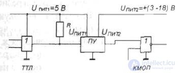

Fig.11.2. Using level converters
As an example, one can cite the widely used level converters СD40109 and HS3374RH (manufactured by TEXAS INSTRUMENTS and INTERSIL).
This class of servicing chips includes level converters for working with various interfaces. So, for example, for the operation of the RS232 serial interface, the logic level 1 should be of the order + 5 ... + 15 V, and the logic level 0 -
-5 ... -15 V. For two-way matching of TTL and RS232 levels, a large number of specialized microcircuits are produced, the most popular of which is MAX232 manufactured by MAXIM, which, in addition to the level converters, contains a +5 V to ± 10 V power converter.
When inputting a signal from mechanical keys, which can be both ordinary buttons and relay contacts, contacts of various sensors, etc., contact bounce occurs, which can cause unwanted element switching (for example, the electronic circuit will perceive multiple button presses instead of once ). A typical solution is the use of an asynchronous RS-flip-flop, the inputs of which are connected via resistors to the power buses (Fig. 11.3).

Fig.11.3. Diagram of eliminating contact bounce
At the first contact of contacts, the trigger will go to the corresponding state and will not react to subsequent contacts with the same contact (the single-pole key cannot oscillate from one contact to another, only “there is contact” - ”no contact” with the same contact ).
When designing an electronic circuit on the FPGA, there are a large number of logic elements, but there are no resistors. In such schemes to eliminate chatter, they use impulse noise suppression circuits that are tuned to the duration of chatter. For the simplest case, the signal reception circuit is shown in Fig. 11.4.
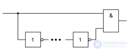
Fig.11.4. The scheme of eliminating bounce and suppression of short impulse noise in a positive signal
In this scheme, a positive signal level (unit level) is sent to the inputs of the coincidence circuit and it is only delayed. If the delay time is longer than the signal duration, then such a signal will not pass to the output of the coincidence circuit. To eliminate contact bounce, the delay value is set longer than the bounce time.
The load of the electronic circuit can be lamps, LEDs, electromechanical relays, high-power contactors and starters. If we are talking about low power devices, they can be controlled directly from typical logic outputs, outputs with increased load capacity, or from open collector outputs (Fig. 11.5).
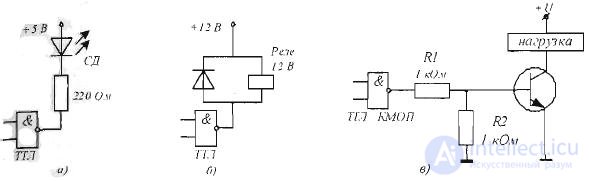
Fig.11.5. Direct control from typical logic outputs
If we are talking about the management of powerful devices powered by a DC or AC circuit, it is necessary to produce galvanic isolation of the circuits and implement stepwise control
(for example, a logic output controls a low-power relay according to 11.5b, this relay, in turn, controls a more powerful relay, etc.). Galvanic isolation is carried out using a relay (Fig.11.5b) or using optocouplers (Fig.11.6).
|
|
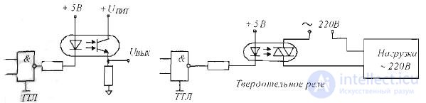
Figure 11.6. Galvanic isolation using optocouplers
The best way to transmit digital signals over short and long distances is to use light transmissions through the optocable. The electrical signal is converted to light by means of an LED or a laser, transmitted through an optocable and received by a photodiode. At the same time, galvanic isolation is naturally carried out and the effect of various kinds of electromagnetic interference on a long transmission line is eliminated. However, in some cases, if there is a slight interference, simpler solutions are used. For example, Figure 8.7a shows the scheme when a signal is transmitted to a line by an open-collector output, and a signal is received by a Schmidt trigger restoring the edges of the signal. To suppress small noise, an RC filter can be used, as shown in Fig.11.7b.
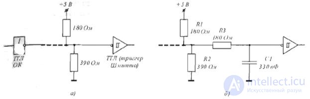
Fig.11.7. Signal transmission directly from the TTL output
Higher noise immunity can be obtained by transmitting a differential signal over a twisted pair, which the differential receiver accepts (Fig. 8.8).
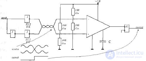
Fig.11.8. Transmit a differential signal over a twisted pair
At the input of the communication line, direct and inverse signals are generated, which are transmitted through it to a differential receiver, which perceives the voltage difference between the inputs, which is equal to 2U signal and does not contain common mode voltage. As a differential receiver in this application, the best results are obtained using instrumentation amplifiers that are specifically designed for this.
To ensure the electrical safety of the equipment and anti-interference, galvanic isolation can be used (Fig. 11.9).
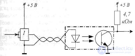
Figure 11.9. Isolation communication line
In practice, in addition to transmission over twisted pair, they also use transmission over coaxial cable (Figure 11.10). A feature of the use of a coaxial cable is the need to harmonize with its characteristic impedance (51 Ohm resistor in Figure 11.10, with a cable impedance of 50 Ohm) and special forming elements (for example, 8T23 and 8T24).
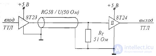
Figure 11.10. Reception and transmission over 50 - Om coaxial cable.
1. Principles of conjugation of TTL and CMOS logic.
2. Using level converters.
3. Diagram of eliminating contact bounce.
4. Direct control from typical logic outputs.
5. Galvanic isolation using optocouplers.
6. Signal transmission directly from the TTL output.
7. Transmission of a differential signal over a twisted pair.
8. The communication line is electrically isolated.
9. Reception and transmission over 50 - Om coaxial cable.

Comments
To leave a comment
Computer circuitry and computer architecture
Terms: Computer circuitry and computer architecture