Lecture
Tile64 processors are designed for use in high-performance network equipment, wireless telecommunications systems, as well as servers for streaming video processing. Allowed to use powerful computing resources in embedded applications with sufficiently low power consumption.
The target circle for these processors is as follows.
Processors are capable of operating in networks with a traffic level of about 10-20 Gb / s, providing support for the following services:
Multimedia applications primarily include digital data processing, easily replacing multiple digital signal processors (DSPs) or FPGAs:
Applications in the field of wireless communications include work in existing GSM / CDMA networks and in next-generation WiMAX & LTE networks. First of all, it is:
The Tile64 processor can be optimized for specific tasks. Theoretically, Tile64 will provide a tenfold increase in performance compared to the Intel Xeon server processor with significantly less power consumption.
Tile64Pro is a general-purpose processor with a MIMD architecture. Each core can operate under its own operating system and under a multiprocessor system such as SMP Linux , respectively, and the processor can simultaneously support various applications, for example, video frame processing, data encryption and network protocol stack processing.
Virtual memory and Tilera's Multicore Hardwall technology allows you to protect data at the kernel level, both for shared memory and for user-level streams and messages.
The processor contains 64 identical computing cells (tile) , organized in a two-dimensional array of 8x8 (Fig.27.1, 27.2). The cell is the base unit of the processor and consists of a combination of a switch and a general-purpose RISC core. Each core is a full-fledged RISC-processor operating at frequencies from 600 MHz to 1 GHz, and contains caches of the first and second levels (L1, L2 cache).
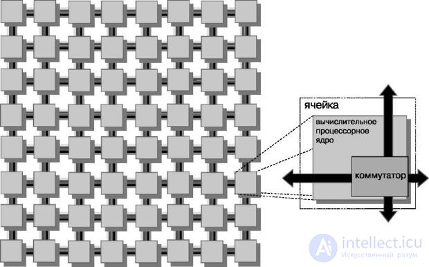
Fig.27.1. Tile64 processor cell
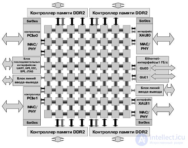
Fig.27.2. Tile64 processor structure
The kernel has all the basic features of a regular processor, such as:
Each of the cores of the Tile64 processor has its own cache memory of the first and second levels (Figure 27.3).
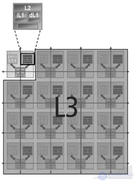
Fig.27.3. Cache organization
The cores are optimized for best performance with minimal power consumption. When working at frequencies between 500 and 1000 MHz, the power consumption is 170–300 mW per core for typical applications. Accordingly, the total power consumption of the processor is about 20 watts.
The coherent cache distributed across the cores provides low latency and high capacity. The cache subsystem consists of a high-performance two-tier non-blocking cache hierarchy. The two-tier solution isolates the first-level cache (L1 instructions and L1 data) from unnecessary memory accesses, keeping the solution fast and energy efficient. Hardware instruction prefetching for instruction cache L1-I reduces the frequency of cache misses. A programmable direct memory access unit allows for extensive data transfer. The processor architecture is designed in such a way that a cache distributed across other cores is available to a separate core. Such an organization of coherent cache provides hardware control over access to shared distributed memory, which allows the kernel to have access to a set of local caches for all other cores, working as a third-level cache.
Organized in this manner, the cache eliminates the bottleneck in accessing global external memory - reduces the frequency of hits.
The system of coherence caches allows you to access the memory page cached by one of the cores, and the rest of the processor cores using read / write operations (similar to accessing the kernel’s own cache). In fact, the kernel, caching data for itself, caches it for all other cores, regardless of their need for this data, which improves the performance of the processor as a whole.
Multicore Hardwall technology allows the user to select one or more cores in a relatively independent processor group, excluding communication between the selected group and other cores that are not included in the group. If a data packet crosses a set group boundary, an interrupt is triggered and control is transferred to the hypervisor, a small, executive-level program for tracking and managing system resources. This ensures the protection of application data in a multitasking environment. The Multicore Hardwall technology protects multiple applications and operating systems from unforeseen interactions and random errors (Figure 27.4).

Fig.27.4. The selection of independent groups of processor cores
The iMesh network provides the high-speed data transfer required to eliminate a system bottleneck and support application scaling. iMesh consists of five separate subnets. The two subnets are completely hardware controlled and used to transfer data between the cores and the memory in case of cache misses or direct memory access. The three remaining subnets are available for applications, allow interaction between the cores and between the cores and I / O devices. A number of abstractions are used to access the hardware, for example, streaming channels similar to sockets, or a messaging interface. The iMesh network allows you to transfer data without stopping applications running on the kernels. This allows the exchange of data between the cores and control and routing for each network connection, including buffering and flow control throughout the network (Figure 27.5).

Fig.27.5. IMesh Network Switch
The switch located near the core is non-blocking and connects the core to the Tilera's iMesh ™ on-chip network, which allows each individual core to interact with nearby cores. The data transfer rate over the iMesh network can reach 27 Tbps.
The network is implemented on topology "thick tree" (Fat Tree).
Development tools include the Tilera's Multicore Development Environment ™ (MDE) environment, which includes standard parallel programming tools for multi-core systems.
Tilera's MDE environment contains:
The iLib library provides software interfaces that allow developers to:
The CSX700 processor architecture was designed to solve the problem of size, weight, and power consumption (Size, Weight and Power (SWAP)), which typically dominates embedded high-performance applications. By integrating processors, system interfaces, and built-in memory with error correction, the CSX700 is a cost-effective, reliable, and productive solution that meets the requirements of modern applications.
The processor is a massively parallel data architecture with a high degree of efficiency and reliability. The architecture is focused on intelligent signal processing and image processing in the time and frequency domains.
The CSX700 crystal contains 192 high-performance processor cores, built-in buffer memory of 256 Kbytes (two banks of 128 Kbytes each), data cache and instruction cache, ECC protection of internal and external memory, and built-in direct memory access controller. To provide the on-chip and inter-crystal network, ClearConnect NoC technology is used (Fig. 27.6).

Fig.27.6. CSX700 processor structure
The external memory interface has 72 bits for monitoring and correcting data (Error Checking and Correction - ECC). Uses 64-bit DDR2 SDRAM memory up to 4 GB. The processor has a 64-bit address space that is mapped to 48-bit physical. Ports CCBR0 and CCBR1 are intended for the formation of multicrystal systems, and can also be used to connect FPGAs.
The processor consists of two relatively independent MTAP modules (cores) containing instruction caches, data, control units of processor elements, and a set of 96 processing cores - processor elements (PE) (Fig. 27.8). Supports simultaneous execution of eight threads.

Fig.27.8. MTAP block structure
At each clock cycle, the processor retrieves the command, decodes it, and sends it to the execution units mono or poly or to the I / O controller. The instruction set is traditional for RISC processors - they are three-address commands. In addition, the processor executes jump instructions and controls thread switching. Commands are executed on mono or poly operands, and some of them are implemented only in a single block (for example, transition commands are only in mono). Each core has a double block of floating-point calculations (addition, multiplication, division, square root calculation, single and double precision numbers are supported), 6 KB of high-performance RAM, and a 128-byte register file. Supports 64-bit virtual address space and 48-bit real.
Processor Specifications:
The on-chip trunk makes it possible to simultaneously perform several exchanges, for example, it provides the processor with access to the internal memory. In addition, it provides the ability to transfer data from external memory to the CCBR0 or CCBR1 ports using the DMA channel.
The cores simultaneously execute one instruction stream in SIMD mode. Data to be processed in parallel is provided with a poly descriptor.
The processor maintains its context for each thread. If the PE cores perform long I / O, then the processor must switch to another thread. In this case, the threads have priorities, and the finished stream with a higher priority interrupts the execution of the stream with a lower one. Threads are synchronized with each other and I / O controllers through hardware semaphores.
Semaphores are special registers whose values are increased or decreased using indivisible atomic commands — signal and wait, respectively. If wait is performed on a zero-value semaphore, the execution of the command is suspended until the signal command is executed on that semaphore in another thread or device. Operations on semaphores are also capable of performing hardware blocks, for example, I / O controllers.
Each PE core may or may not execute instructions, depending on the value of the enable bits. If all of these bits are "1", then the command is executed. If at least one of these bits is equal to "0", most of the commands are not executed (except, for example, commands for changing the state of the enabling bits). The enable bits register is treated as a stack: the bits enter it through the top.
Conditional execution of commands in PE is supported by poly transition commands: if, else, endif, etc. They control the values of the enable bits. For example, when the if command is executed comparing two operands in all PEs, the following happens: in PEs where there is a match, “1” will be placed at the top of the stack, and in those where a match is found, “0” is placed at the top of the stack. Accordingly, these PEs will or will not execute subsequent commands — up to the endif command, which will “push” the value entered by the if command from the stack. The stack has a fixed size, so you need to monitor its overflow.
Commands for reading and writing from local memory PE to registers can also be executed or not, depending on the value of the enable bit. For the unconditional execution of the exchange between memory and registers, special commands were introduced forced load and forced store.
The PE I / O channel includes a controller and one or more direct access channels. The controller interprets I / O commands and interacts with threads through semaphores. The exchange between local PE memory and external devices is performed by programmable I / O or using direct access channels to local memory. Each processor can read its part of the data or perform a general reading - with the "cutting" of the same blocks for each processor.
Processor elements (PE) are able to exchange with the "neighbors" on the right and left. At each clock cycle, PE can transfer from its register to the left or right neighbor register and receive data to its registers simultaneously to the right and left. Shift commands are used to the right and to the left, as well as the transfer to "neighbor". If PE has the enable bit "0", then the neighboring processor cannot change the state of its registers.
Designed for low-power systems, this processor combines a clock speed control that is common to embedded systems with a relatively low clock frequency. Frequency control allows you to adjust the performance of applications when working in conditions of specific power consumption and thermal environment.
The CSX700 is supported by a professional development environment (SDK) based on Eclipse technology with visual debugging tools based on an optimized ANSI C compiler with extensions for parallel programming. In addition to the standard C library, there is a set of optimized libraries with functions such as FFT, BLAS, LAPACK, etc.
The 167-core computing platform (hereinafter referred to as the processor), developed at the University of California, Davis, is implemented in silicon by the STMicroelectronics company over a 65-nm technological cycle. This processor is designed primarily for digital signal processing, communication functions, multimedia applications. The processor contains 164 programmable cores with dynamic control of the supply voltage and a clock frequency, three specialized processors, three shared memory buffers of 16 KB each. All components of the processor are clocked by their own independent generators and connected by a special on-chip network. The block diagram of the processor is shown in Fig.27.9. Each of the cores has 16-bit data buses, a 40-bit battery, an independent clock generator with the possibility of stopping.
Each core has a command memory of 128 35-bit words, 128 words of a 16-bit data memory, two 16-bit FIFO buffers of 64 words each, and a single-output six-level RISC pipeline. RISC-cores support more than 60 basic instructions, including byte addition / subtraction, the calculation of the minimum / maximum and absolute values, transitions, returns from subroutines, conditional execution instructions, cycles, a block with a floating point. The task of calculating the square root (CORDIC) is performed in 216 cycles.
The FFT processor can dynamically switch between calculating the direct and inverse Fourier transforms with the number of samples from 16 to 4096 by calculating a complex 4-point or 2-point "butterfly" per cycle.
A configurable Viterbi processor contains 8 ACS modules and can decode codes up to length 10.
The motion detection processor supports several fixed and programmable search algorithms that meet the H.264 algorithm, and performs over 14 billion operations (SADs) per second at a frequency of 880 MHz.
The processor cores exchange data through configurable connections between neighboring processors and long connections. Connections are cyclically switchable and statically configurable, which is in good agreement with the local synchronization technology used in the processor.
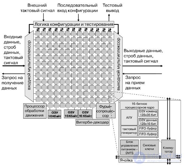
Рис.27.9. Структурная схема 167-ядерного вычислительного массива
Структура связей включает два входа вычислительного ядра и одиночный выход, который динамически подключается к восьми выходам ячейки. Каждая связь содержит 16-разрядную шину данных, сигнал синхронизации источника, разрешающий сигнал (стробирующий) и сигнал запроса на смену направления, используемый для контроля потока. Ограниченные только искажениями тактового сигнала, связи могут быть сконфигурированы для передачи данных сквозь процессор в выбранном выделенном канале без привлечения промежуточных процессоров и безотносительно их текущих напряжений питания и тактовых частот (рис.27.10). Данные могут быть помещены в конвейер в каждой ячейке для достижения полной скорости при передачи на длинные расстояния или передаваться напрямую, если дистанция мала или тактовая частота источника данных мала . Такие меры снижают общую задержку передачи данных.
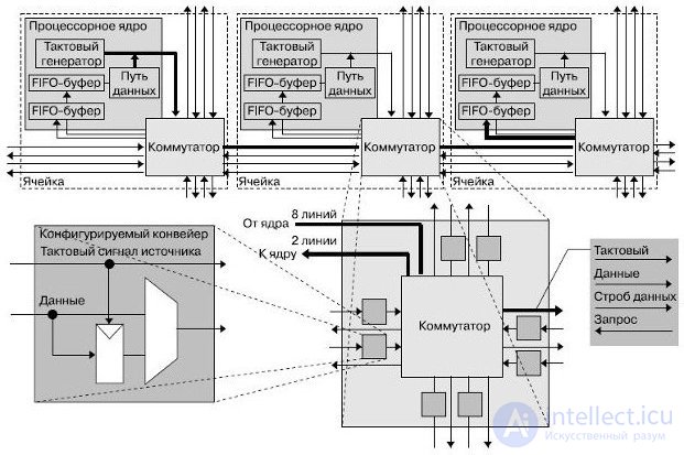
Fig.27.10. Example of internuclear compounds
To reduce energy dissipation, when the cores are not fully loaded, the cores can change their own supply voltage and clock frequency. The cores change the supply voltage by connecting their power leads (VddCore) to one of two global power buses. It is also possible to disconnect VddCore lines of unused processors from the supplying global buses (thus reducing the core consumption by more than 100 times).
The power consumption of a single core with a full load at 1.07 GHz and 1.2 V power supply is about 48.4 mW. With a supply voltage of 0.675V, the cores operate at 66 MHz and consume 0.61 mW. Thus, depending on the mode, the power consumption of the processor as a whole ranges from 101 mW to 7.93 watts.
According to the test results, a 9-processor JPEG encoder operating at 1.3 V and 0.8 V supply voltages reaches approximately 8% energy savings compared to the same encoder that works exclusively with 1.3 V. The receiver is fully compatible with the IEEE 802.11a / g standard, implemented using 39 processor cores (only connections between neighboring cells are involved), plus specialized FFT and Viterbi processors. Using long connections, the receiver can be implemented on 27 cores - almost a third less. When simulating, the latest receiver version dissipates approximately 75 mW when operating at 690 MHz and data rates of 54 Mb / s in real time (including 2.7 mW for the FFT processor and 5.5 mW for Viterbi).
Процессор Cell представляет собой мощную асимметричную многоядерную процессорную систему. Состоит из процессорного элемента Power, чаще всего выполняющего управляющие функции, и из восьми синергичных процессорных элементов, выполняющих основную вычислительную работу. Ядра объединены при помощи двунаправленной кольцевой шины.
Для борьбы с узким местом при доступе в основную память в процессоре Cell в процессорном элементе PPE применяется двухуровневый кэш и аппаратная поддержка двух потоков. В элементах SPE присутствует локальная оперативная память объемом 256 Кбайт и высокопрозводи-тельный блок прямого доступа в память.
Процессор Cell — совместная разработка компаний Sony, Toshiba и IBM, которые организовали альянс, известный как «STI». Разработка архитектуры и первые прототипы были созданы в STI Design Center за четырехлетний период с начала марта 2001 года.
Первое коммерческое применение процессора Cell — в игровой консоли Sony PlayStation 3. Toshiba использует Cell в своих домашних HDTV-кинотеатрах.
С 2006 года компания IBM выпускает блэйд-сервер QS20, оборудованный двумя процессорами Cell BE. Модули QS22, оборудованные двумя процессорами PowerXCell 8i (модифицированная версия Cell BE с аппаратной поддержкой вычислений двойной точности), используются в суперкомпьютере IBM Roadrunner .
Specifications
В настоящее время выпускается процессор третьей ревизии PowerXCell 8i — изготовление идёт по 45 нм техпроцессу. PowerXCell 8i по сравнению с предшественником обладает в пять раз более высоким быстродействием при выполнении операций с плавающей запятой с удвоенной точностью.
Cell представляет собой процессор с архитектурой CBEA (CBEA (Cell Broadband Engine Architecture) — архитектура, расширяющая 64-битную архитектуру), построенный на основе 64-битной архитектуры Power, которая направлена на распределенную обработку данных и выполнение приложений, предназначенных для обработки больших объемов мультимедиа-данных (рис.27.11).
Процессор состоит из набора модулей, объединенных при помощи высокоскоростной шины (EIB), которая представляет собой две пары колец (96 байт за такт), работающих на половине частоты процессора. Пропускная способность канала ввода данных — 35 Гб/с, канала вывода данных — 40 Гб/с, объединенная пропускная способность канала обмена данными с общей памятью — 25,6 Гб/с.
В состав процессора входит 8 одинаковых процессорных модулей (SPE), содержащих процессорное ядро (SPU), локальную память модуля (LS), один процессорный модуль (PPE), содержащий 64-битный процессор, кэши первого и второго уровней, два реконфигурируемых некогерентных интерфейса ввода-вывода (BIC), интерфейс памяти (MIC).
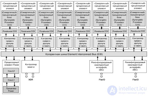
Рис.27.11. Блок-схема мультипроцессора Cell
Процессорный элемент Power (PPE) имеет 64-разрядную архитектуру, с упорядоченной выдачей двух инструкций одновременно (SMT), кэш данных и кэш инструкций первого уровня объемом 32 Кб, объединенный кэш второго уровня объемом 512 Кб.
Процессор обеспечивает два одновременных потока выполнения и может рассматриваться как двухпроцессорный мультипроцессор с общим потоком данных. Ядро чередует команды от двух вычислительных потоков, выполняющихся одновременно. Это позволяет программному обеспечению воспринимать его как два независимых процессора. Продублированы все видимые состояния, в том числе видимые регистры и регистры специального назначения (за исключением регистров, имеющих дело с ресурсами на уровне системы, такими как логические разделы, память и управление потоками). Такое решение позволяет оптимизировать применение слотов выдачи команд, сохранить максимальную эффективность процессора и уменьшить глубину конвейера. Невидимые для программиста ресурсы (типа кэшей и очередей) обычно используются обоими потоками совместно. Исключение составляют те случаи, когда ресурс невелик или может существенно повысить производительность многопоточных приложений.
Простые арифметические операции выполняются и отправляют далее свои результаты за два такта. Задействован режим отложенного выполнения на конвейере операций с фиксированной запятой, благодаря чему команды загрузки также завершаются и отправляют свои результаты за два такта. Команда двойной точности с плавающей запятой выполняется за десять тактов.
PPE поддерживает обычную иерархию кэш-памяти; имеются кэши первого уровня для команд и данных емкостью по 32 Кбайт и кэш-память второго уровня емкостью 512 Кбайт. Кэш второго уровня и кэши преобразования адресов используют таблицы управления заменой, чтобы разрешить программе направлять данные из определенных диапазонов адресов в конкретное подмножество кэша. Такой механизм позволяет блокировать данные в кэше, если размер диапазона адресов равен размеру множества. Он может служить и для предотвращения перезаписи данных в кэше: данные, применяемые только один раз, направляются в определенное множество кэша. Все это повышает эффективность процессора и усиливает контроль над процессором, осуществляемый в масштабе реального времени.
Процессорный блок состоит из 3 блоков: IU (Instruction Unit); XU (eXecution Unit); VSU (Vector Scalar Unit) (рис.27.12). Узел команд IU (Instruction Unit) отвечает за выборку, дешифровку, выдачу и завершение команды, а также за выполнение команд перехода. Узел операций с фиксированной запятой XU (Fixed-Point eXecution Unit) выполняет все команды с фиксированной запятой и команды загрузки/сохранения. Узел векторно-скалярных команд VSU (Vector Scalar Unit) отвечает за векторные команды и команды с плавающей запятой.
Узел команд IU за один такт выбирает из каждого потока четыре команды в буфер команд и отправляет команды из этого буфера по назначению. После дешифровки и проверки зависимостей команды выдаются на узел выполнения по две за такт. Для прогнозирования результата команды перехода служит таблица истории переходов 4 Кбит х 2 бит с шестью битами глобальной истории на поток. Узел IU может выдавать до двух команд за такт.
При такой "сдвоенной" выдаче возможны любые комбинации, кроме двух команд к одному и тому же узлу, а также следующих исключений. Простая векторная, комплексная векторная, векторная с плавающей запятой и скалярная с плавающей запятой арифметические команды не могут быть сдвоены с командой того же типа (например, не допускается выдача простой векторной команды в одном такте с комплексной векторной). Однако эти команды могут быть сдвоены с любой формой команды загрузки/сохранения, перехода с фиксированной запятой или перестановки элементов вектора. Очередь готовых к выдаче команд в узле VSU отделяет конвейеры векторных команд и команд с плавающей запятой от остальных конвейеров. Это позволяет выдавать такие команды вне очереди других команд.

Рис.27.12. Структурная схема процессорного элемента PPE
Узел XU состоит из двух файлов регистров общего назначения 32x64 бит (по одному на поток), блока выполнения команд с фиксированной запятой и блока загрузки/сохранения. В последний входят кэш данных первого уровня, кэш преобразования адресов, 8-элементная очередь кэш-промахов и 16-элементная очередь хранения. Он поддерживает неблоки-руемый кэш данных первого уровня, который позволяет процессору обращаться к другой области кэш-памяти даже в процессе замены блока, вызвавшего кэш-промах (hit under miss cache).
The VSU node consists of two register files of 32x64 bits (one per stream) and a double precision pipe with ten stages. The node works with a 128-bit data stream. It has four nodes for performing simple and complex vector operations, single-precision floating-point operations, and permutation operations. It has two 32-element 128-bit vector file registers (one per stream), and all commands are 128-bit SIMD commands with varying widths of elements (2x64, 4x32, 8x16, 16x8 and 128x1 digits).
SPE (Synergistic Processor Elements) is a separate processor that runs a separate application, but shared coherent memory and a large set of commands for the DMA allows you to organize effective data exchange between SPEs (Fig. 27.13).
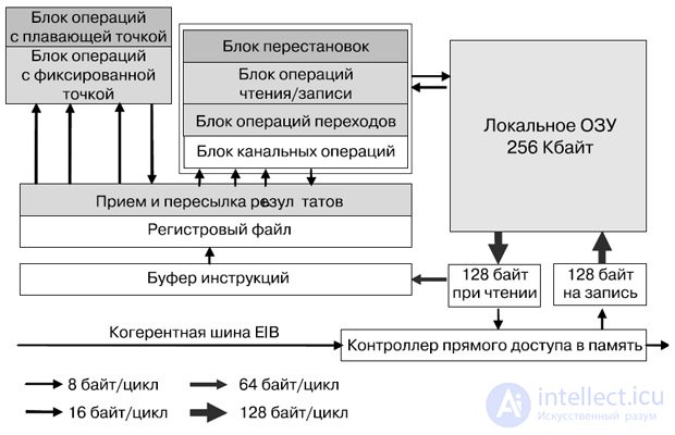
Fig.27.13. Block diagram of the processor element SPE
The selection of instructions and loading / saving instructions work only within the address space of the local SPE memory. The large volume of the register file serves to more fully fill the computing pipeline. Each SPE has a Memory Flow Controller (MFC) that includes a DMA controller.
SPE can configure DMA to exchange data with the local memory of another SPE, as well as to exchange data with shared memory.
The SPE processor element implements a new command system architecture, power consumption and performance of which are optimized for computing and multimedia applications. SPE works with 256 KB local memory that stores commands and data. They are transferred between this and system memory using asynchronous coherent direct access commands, which are executed by the flow control unit that is part of any SPE.
Each SPE supports up to 16 pending direct memory access (DMA) commands. These coherent commands use the same addresses as in PPE, address translation and security, managed by page tables and segments from the Power Architecture, so addresses can be transferred between PPE and SPE. As a result, the operating system is able to use shared memory and consistently manage all system resources.
A DMA block can be programmed in one of three ways: using SPE commands that insert DMA commands into queues; by preparing in local memory a list of commands for sending the contents of scattered parts of memory (scatter-gather DMA) and issuing a single list of DMA commands; by inserting commands into the DMA queue of another processor (with appropriate privileges) and applying save or write DMA commands. For ease of programming (to allow DMA transactions like "local memory - local memory") local memory is mapped onto the processor's memory card. However, when caching this memory is not coherent in the system.
The emergence of local memory introduces a new level of memory hierarchy - in addition to the registers that provide local data storage in most processor architectures. This provides a mechanism for dealing with the "memory wall" problem, since it allows you to simultaneously perform many memory transactions without deep speculation, which greatly reduces the efficiency of other processors. The latency of the main memory is close to 1,000 clocks, so the few clocks that are needed to set up a DMA command when accessing it become an acceptable additional load. Obviously, such an organization of the processor is convenient for processing multimedia streams. And since local memory is large enough to store more than just the kernel (streaming kernel) of a stream, support for a variety of programming models is possible.
Local memory is the largest component of SPE, so its effective implementation was very important. To minimize the area used single-port cell SRAM. Local memory has narrow (128-bit) and wide (128-byte) read and write ports. This provides high performance, although it must act as an arbiter in relation to read, write, select, load, and save operations with direct access. The wide port is used for direct reading and writing to memory, as well as for pre-fetching commands.
Since a typical 128-byte direct read / write operation requires 16 processor cycles to transfer data on the internal coherent bus (even when direct read / write operations are performed without bandwidth restrictions), seven out of every eight cycles remain available for load, store, and selection of commands. Similarly, commands are selected 128 bytes at a time, and the load on the local memory remains minimal. The highest priority is given to the DMA commands, followed by the load and save operations, and the pre-fetch operation of the command is performed when there is a free clock. There is a special command "without operation", which allows, if necessary, forcibly ensuring the availability of the slot for selecting a command.
The execution units in SPE operate on a 128-bit data stream. A sufficiently large register file of 128 elements allows the compiler to reorder the commands and compensate for the latency of their execution. There is only one register file, and all commands are 128-bit SIMD commands with variable element widths (2x64, 4x32, 8x16, 16x8, and 128x1 bits).
Up to two teams can be issued per clock; one slot for issuing a command supports floating-point and fixed-point operations, and the other provides load / save, byte swap and jump operations. Simple fixed-point operations take two clocks, and single-precision floating point commands and load commands require six clocks. Dual-precision double-stream floating-point SIMD commands are also supported, but the maximum speed of issuing them is seven clock cycles per command. All other commands are fully pipelined.
In order to limit the additional load on equipment caused by branch prediction, a programmer or compiler can "prompt" the transition. The transition prompt command notifies the equipment of the address of the upcoming transition command and its target address. The hardware (assuming that local memory slots are available) preselects at least 17 commands at the destination of the transition. To reduce the number of branches in the code, you can use a bitwise select command with three sources.
Configuring the DMA controller as well as the presence of request queues allows SPE to work in parallel with the operation of DMA. This is the way to avoid idle SPE as a result of a delay in receiving data from main memory.
Although PPE and SPE share a common memory, there is a clear separation of functions between them. The PPE is optimized for solving control problems and changing context, while SPE is for solving computational problems.
The PPE accesses the shared memory through load / store instructions (via the cache hierarchy), moving data between the PPE register file and the main memory.
SPE accesses shared memory via DMA transfers that transfer data between local SPE memory and shared CELL memory.
The ATAC architecture is based on the cellular principle of building multi-core processors, with the difference that the cells in this case are clusters that consist of several computing cores connected by a nanocrystal network. The cells are combined by a broadcast optical bus. An interesting point is the integration of optoelectronic modules and optical channels in the framework of CMOS technology. The possibility of scaling the number of cores to several thousand.
The direction of development of modern microprocessors is quite understandable - a gradual transition to multi-core systems. Many manufacturers claim to reach 1000 or more cores on a chip by about the middle of the next decade (∼2015). But there is a problem: the current processor architectures, and especially the inter-core communication mechanisms, are poorly adapted to scaling up to a thousand cores. The same applies to the methods of their programming.
The ATAS architecture combines an optical broadcast network with a mesh (tiled) multi-core architecture to significantly increase performance, energy scalability and simplify programming.
Existing multi-core architectures do not allow Moore's law to be followed for some important classes of parallel applications. Restrictions are imposed by the cost of nuclear interactions and the exchange rate with external memory. The goal of the ATAS project is to solve these problems by introducing optical communication technology.
A computational process can be thought of as a kind of information flow that captures the processor core, the distribution of instructions, and the transfer of values between cores. As the number of processors increases, the data transfer delay between distant cores will increase. The effect may increase if the interaction between pairs of cores will require already occupied communication resources. This is important for applications running on global interactions (broadcast or synchronized caches). In addition to loss of productivity, global communications operations also lead to significant energy costs. Multiprocessors with a small number of cores use a bus for internal connections. This simple solution, as you know, does not scale to a large number of cores. Systems with a large number of cores use point-to-point communications, where communications are managed programmatically.
As a rule, for applications with an irregular, unpredictable or predictable link structure, the transition to processors with thousands of cores on a chip can be extremely difficult or impossible. The scalability of applications is also hampered by existing software techniques. Programmers must distribute the calculations over space and over time, and also manage the interaction of the cores if they want to achieve high performance for a given hardware architecture. Depending on the on-chip network used, coordinating the actions of hundreds and thousands of processors can be extremely difficult.
Actions such as delivering instructions to kernels can create difficulties even for SIMD architectures. Existing programming techniques do not provide for optimizing interprocessor communications to achieve high performance. Broadcast and all-to-all messages used in synchronization, negotiation, or instruction distribution protocols do not have direct hardware support and are emulated by multiple point-to-point transmissions.
The ATAS processor architecture provides a solution to these problems by organizing an optical network instead of electrical channels and buses. The project aims to integrate optoelectronic components with standard CMOS circuits. ATAC provides for frequency multiplexing - transmission of signals at different wavelengths - up to 64 frequency separated channels. Optical lines, among other things, transmit data at higher speeds than electric lines (a function of the refractive index of light in comparison with the delays of RC circuits, the dielectric surrounding the connections, and the delay necessary for relaying an electrical signal).
Optical signals may also require less power than electrical signals (especially for long distances), due to lower losses and no need to repeat signals.

Fig.27.14 ATAS-architecture
The ATAS architecture (Fig. 27.14) is based on the ability of nano-optics to create high-performance, global crystal networks with low signal propagation delays. The network consists of an optical channel covering the crystal. Optical hubs transmit data by modulating the laser beam of the source and directing it to the network. The light quickly spreads through the channel and becomes available for reception to the other hubs. Thus, any message on the network can be effectively transmitted to all its members. Filtering on the receiving hub allows you to limit the number of recipients of the message.
ATAS allows for a new programming paradigm for multi-core systems, with a large number of shared data and a simple instruction distribution mechanism within the SIMD model. The broadcasting mechanism allows massed coordination of caches of many cores with almost no restrictions.
When using new ATAS optical technologies, the processor has the potential to reduce the difficulty of programming, increase energy efficiency, increase the throughput of both external and internal data buses, and accordingly provides for power scaling.
The key elements of the technology present in ATAS are: the so-called "optical power source" - a light source, waveguides for transmitting light, modulators for placing light signals into waveguides, detectors for receiving signals. In ATAS, the source of light (optical power) is external lasers. The luminous flux is directed to the nacrystal fibers. The power consumption of the external laser is approximately 1.5 W with an output of approximately 0.2 W in the form of optical radiation entering the light guide. To use a frequency separation scheme, it is assumed that there are several sources of laser radiation. Light guides are built-in channels through which light travels. They direct and distribute by combining a material with a high refractive index in the center and with a smaller edge of the channel. The fibers can be made of both silicon and polymer. Taking into account the fact that silicon fibers can be placed on a crystal more compactly and that the modulators for a silicon fiber are much more compact than for a polymer fiber, it is supposed to create silicon fibers in ATAS. Moreover, silicon fibers can be manufactured in a standard CMOS process.
Optical fibers with losses of less than 0.3 dB / cm and a capacity of at least 10 mW are required. Both requirements are achievable in silicon. The following components are used to exchange information: a light source, a modulator, an optical filter, and an electronic modulator driver. The optical filter is a ring resonator (Fig.27.15), tuned to a specific wavelength - determined by the size of the resonator (it also determines the distance between the wavelengths for the WDM scheme). Further adjustment can be made by changing the temperature of the resonator or its charge. A modulator is an optical device that generates a digital signal by changing the absorption coefficient. Modulators are used to convert an electrical signal into an optical signal — a kind of optical switch that places an optical signal into a fiber.
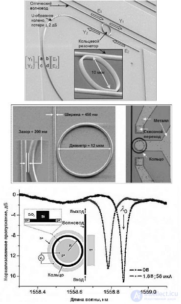
Fig. 27.15. The structure of the ring optical resonator
The modulators required for the ATAS architecture should have parameters that will approximately be achieved in 2012: switching losses - 1 dB, area - less than 50 square meters. μm, the modulation rate is 20 Gb / s, the switching energy required is less than 25 fJ and the total consumption is about 25 μW / GHz. At the receiving side, an additional component is used to receive the signal - an optical filter to receive the signal and convert it to an electrical form.
An optical filter (ring resonator) is used to extract light of the desired wavelength from the optical fiber and transport it to the photodetector. Like the modulator, the optical filter must be tuned to a specific wavelength. The photodetector in this case should be an ultra-sensitive receiver. The architecture of ATAS requires the following parameters: for 11-nm process technology - sensitivity is more than 1 A / W, bandwidth is more than 3 dB at frequencies more than 20 GHz, occupied area is less than 20 kV. mkm, parasitic capacitance less than 1 fF. With this technology, the output of the detector needs to be amplified. As a rule, starting with 22 nm technology, a smaller transistor input capacitance allows a photo detector to control digital circuits. In Figure 27.16, the above components are depicted together. For one core, the transmitting part is shown, for the other, the receiving part.
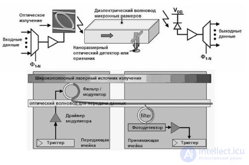
Рис.27.16 Схема оптической передачи между двумя ядрами
Для всех ядер, входящих в архитектуру, узлы приема-передачи оптических данных одинаковые. Сигналы модулятора используются для посылки 0 или 1 в сеть. Драйвер модулятора состоит из нескольких инверторов, которые управляют емкостной нагрузкой модулятора. Модулятор помещает свет на волне предварительно настроенной длины в световод, кодируя тем самым 0 или 1. Оптически кодированные данные распространяются по световоду на скорости, равной примерно одной трети скорости света, и принимаются фильтром, настроенным на ту же длину волны. Кванты света улавливаются приемником и передаются приемному регистру на приемной стороне.
Архитектура АТАС представляет собой "плиточную/ячеистую" многоядерную архитектуру, сочетающую технологию электрических соединений с оптической накристальной сетью. Применяется связанный двумерный массив простых вычислительных ядер, каждое из которых содержит одиночный или двойной RISC-процессор и кэш данных первого уровня. ATAC использует протокол распределенных директорий. Часть распределенной директории расположена в каждом узле.
Ядра в АТАС связаны двумя сетями — электрической EMesh и оптико-электрической ANet. ENet — обычная двумерная электрическая сеть типа "точка-точка", аналогичная существующим в обычных мультипроцессорах. EMesh идеальна для предсказуемых, близких взаимодействий. ANet предлагает технологию для организации оптической накристальной сети, основанную на технологии оптической памяти. Ядро сети ANet составляет ONet (рис.27.17). Сеть ANet содержит 64 оптически соединенных кластера, включающих в себя небольшие электрические структуры, служащие для взаимодействия с оптической сетью, — это сети ENet и BNet.
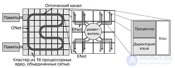
Рис.27.17. Организация связи между модулями АТАС архитектуры на различных уровнях
ANet используется обычно для осуществления передачи данных между удаленными ядрами или для глобальных передач в рамках сети (широковещательные передачи).
Ключ к эффективной организации глобальных коммуникаций в пределах кристалла — оптическая сеть ONet. Она обеспечивает связь между отдельными конечными точками, называемыми хабами. Хабы соединены между собой световодом, проходящим через весь кристалл, формируя замкнутое кольцо (рис.18.33). При помощи модулятора, оптических фильтров и приемника хаб имеет возможность передавать и принимать данные из световодов. Сигнал, посланный одним из хабов, быстро достигает остальных. Таким образом, любая передача в сети может быть широковещательной. Для передачи независимых данных применяется частотное мультиплексирование каналов. Каждый хаб имеет фильтры, настроенные на уникальную длину волны, и фильтры, позволяющие ему принимать сигналы на всех длинах волн. Эта возможность используется при организации глобальных передач, синхронизации ядер, управлении сетью. В дополнение к этому повышенная скорость передачи исключает разнородную задержку распространения сигнала, зависящую от расстояния между ядрами, — в любой паре хабы взаимодействуют между собой с малой фиксированной задержкой, вместо задержки на один цикл на узел в связях типа "точка-точка". В общем, функциональность сети ONet можно сравнить с полносвязной сетью с двунаправленными связями между узлами и с дополнительной функцией широковещания. Частотное разделение каналов позволяет задействовать один световод для нескольких перекрывающихся передач в различных направлениях (для сравнения, электрическая связь обычно используется для передачи одного бита). Для многих сетевых операций, трудно реализуемых в электрических сетях, применение АТАС существенно увеличивает эффективность. ONet может масштабироваться до как минимум 64 хабов (возможно до 100). Количество длин волн, на которые могут быть настроены фильтры, ограничено минимально необходимым расстоянием, спектральной шириной канала и общей шириной полосы излучения в питающем световоде. Также существуют ограничения по общему количеству энергии, которое может передать световод в отношении к количеству энергии, требуемому детектором для приема сигнала, и по максимальной длине волновода, зависящей от потерь распространения.
Указанные ограничения могут быть обойдены использованием нескольких волноводов и распределением каналов передачи данных между ними. Как правило, при этом площадь, необходимая для реализации световода, может также стать ограничением. Оптические компоненты сети и сама сеть могут быть вынесены на отдельный уровень КМОП-стека и накладываться на электронные компоненты, к которым они подключаются. К примеру, на кристалле площадью 400 мм 2 может разместиться оптическая сеть с 384 хабами. Для рассматриваемого случая ONet соединяет 64 одинаковых кластера при помощи 64-битной оптической шины, проложенной по всему кристаллу. Каждый кластер содержит 16 вычислительных ядер и хаб сети ONet. Внутри кластера ядра связаны между собой и с оптическим хабом двумя сетями — ENet и BNet. ENet используется только для передачи данных от ядер кластера к хабу ONet. BNet — широковещательная электрическая сеть для передачи данных от оптической сети вычислителям.
Более детально процесс передачи данных с применением сети ANet показан на рис. 27.18.

Рис.27.18. Процесс передачи данных с использованием сети ANet
Сообщения ядер достигают хаба, который, в свою очередь, пересылает их в сеть ONet на своей уникальной длине волны. Это позволяет двум хабам передавать данные одновременно без интерференции. ONet состоит из нескольких световодов: 64 для данных, 1 для управления и несколько для метаданных. Световоды метаданных служат для указания типа передаваемого сообщения (чтение памяти, данные и пр.) или как тэг сообщения (для устранения двусмысленности при нескольких сообщениях от одного источника). Хаб приемника принимает оба значения последовательно в FIFO-буфер, связанный с конкретным отправителем. Затем данные пересылаются вычислительным ядрам через BNet. Оптическая часть позволяет эффективно реализовывать широковещательную передачу с большей скоростью и меньшими затратами на регенерацию сигнала.
Ядра в АТАС — простые процессоры с кэшем данных и команд первого уровня. Когерентность кэшей поддерживается при помощи протокола, известного как ACKwise. Кэши поддерживают когерентность при помощи протокола распределенных директорий MOESI.
Директории распределены равномерно между ядрами, более того, каждое ядро является "домом" для определенного пула адресов (распределяется статически). Рис 27.19 представляет три ядра, находящиеся в различных кластерах. Каждое ядро содержит процессор, кэш данных и директории кэша. Для примера (рис. 27.19) предположим, что обращение к директории кэша всегда приводит к промаху (необходимости синхронизации кэша). Стрелками на рисунке обозначены типовые операции по согласованию кэшей: промах по записи по адресу А ядром а. В данном примере ядро б является "домом" адреса А, и начальное состояние адреса А в кэше — "занято" (O-state) ядром с. Трафик по согласованию кэшей передается по сети ANet. Последовательность действий для согласования кэшей для данного случая будет следующей:
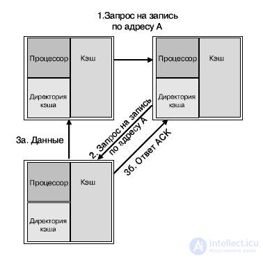
Рис.27.19. Пример согласования кэшей различных ядер
1. процессор в ядре а пытается осуществить запись по адресу А и получает ошибку записи;
2. ядро а посылает запрос на запись ядру б, к которому относится адрес А;
3. ядро б не имеет данных в кэше, но указывается, что этот адрес занят ядром с. Ядро б посылает запрос на запись по этому адресу от имени ядра а;
four.
o ядро с пересылает данные адреса А ядру а и обновляет состояние кэша для этого адреса до "недействительный";
o ядро с посылает ACK-сигнал в директорию ядра б;
5. линия кэша, содержащая адрес А, обновляется на ядре а, и линия получает статус "модифицирована";
6. процессор ядра а производит запись по адресу А.
Когда ядрам необходимо обратиться к внешней памяти, они делают это при помощи нескольких встроенных в кристалл контроллеров памяти. Каждый контроллер памяти замещает кластер ядер и, таким образом, имеет свой выделенный оптический хаб. После получения запроса по оптической сети он обращается к внешним DRAM-модулям посредством стандартных линий ввода-вывода. Результаты передаются в оптическую сеть. Изменяя количество контроллеров памяти и количество кластеров, можно на различных АТАС-процессорах достигать различных значений показателей пропускной способности подсистемы памяти и вычислительной мощности. Основная задача контроллера памяти — преобразовать запросы от процессорных ядер в транзакции на шине памяти. Выбор технологии шины, таким образом, не зависит от архитектуры накристальной сети.
Вполне допустим вариант использования оптических интерфейсов как на ввод-вывод, так и для шины памяти. Это даст преимущество в пропускной способности и потребляемой мощности.
Каждый оптический вывод может поддерживать до 64 длин волн со скоростями до 20 ГГц. Скорость передачи данных будет ограничена скоростью работы электронных компонент, управляющих оптическим потоком. Предполагается, что скорость в 5 ГГц вполне может быть достигнута. При этом полоса пропускания оптического вывода может достигать 320 Гб/с (40 Гб/с). Для сравнения, 64-битная DDR3 имеет пиковую пропускную способность 12,8 Гб/с. Поскольку оптическая шина памяти состоит только из одного световода, уменьшается количество выводов, и это при увеличении пропускной способности практически в три раза. Все это де- лает применение оптического ввода-вывода востребованным для АТАС- процессоров с несколькими контроллерами памяти.
Архитектура ориентируется на 11-нм техпроцесс, который, по мнению ее разработчиков, может быть реализован к середине десятилетия (ориентировочно 2012-2016 гг.).
1. Структура процессора Tile64.
2. Организация кэш-памяти в процессоре Tile64.
3. Коммутатор сети iMesh.
4. Структура процессора CSX700.
5. Структура MTAP-блока в процессоре CSX700.
6. 167-ядерная вычислительная платформа — AsAP-II.
7. Общая структура процессора Cell.
8. Структурная схема процессорного элемента PPE в Cell.
9. Структурная схема процессорного элемента SPE в Cell.
10. Альтернативная технология построения многоядерных систем на кристалле — ATAC.
11. Основные идеи архитектуры ATAC.
12. Ключевые элементы технологии АТАС.
13. Структура межъядерных связей в архитектуре АТАС.
14. Передача данных и согласование кэш-памяти в архитектуре АТАС.

Comments
To leave a comment
Computer circuitry and computer architecture
Terms: Computer circuitry and computer architecture