Lecture
Thyristors
Thyristor is a semiconductor device based on a single crystal with a four-layer structure with three pn junctions and having valve properties, i.e. a device that allows current to pass in one direction with the ability to control its average and effective value by controlling the thyristor on phase.
Thyristor designation
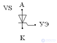
The control electrode allows you to control the moment of thyristor on, even with a positive potential difference between the anode and cathode, less breakdown, if through the 1st pn junction to create a direct current. The moment of activation, or the phase of inclusion, is called the control angle .
Thyristor classification:
• Dinistor, without control electrode; only anode and cathode
• Trinistor, with control electrode
• Semistor, bidirectional thyristor.
Principle of operation
Consider the principle of operation of the thyristor.
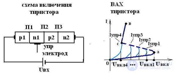
When a voltage Uin is applied to the thyristor anode, the P1 and P3 transitions are open, and the P2 transition is closed, therefore all input voltage is applied to the locked layer P2. As a result, the thyristor current is very low. As the input voltage increases, the current through the thyristor will increase slightly until the P2 junction breaks through is called the turn-on voltage
Uin = Uprob = Uvkl (point a). Segment | 0a | this is the reverse branch of the P2 junction. During the breakdown of the P2 transition, the current through the thyristor sharply increases (point b). Segment | Sun | All three transitions are under the input voltage, since the voltage of the transitions P1 and P3 are the same, but opposite in sign. Segment | ac | - plot of "negative" thyristor resistance.
If current is applied to the control electrode, then the thyristor breakdown voltage can be changed. The greater the control current, the lower the turn-on voltage of the thyristor, i.e. thyristor, turn on earlier.
Iupr4> Iupr3> Iupr2> Iupr1> 0, therefore Uvkl4
Thyristor parameters:
• Uvkl - inclusion voltage
• Ivr - control current
• Uupr - control voltage
• t on - on time
• toff - off time
• Uon max, with Ipr = 0
An important parameter of the thyristor is the control current I, the current of the control electrode, which ensures that the thyristor switches to the open state.
Thyristor virtues
Thyristors are widely used due to a number of advantages compared with diodes:
• high power density
• low internal losses, i.e. high efficiency
• wide range of operating temperatures (from –40 to +120 ° C)
• instant readiness for work
• short unlocking and restoring of locking properties
The industry produces thyristors
• on currents I from 2 to 150A
• for voltage U from 50 to 1000V
The current version of the page has not yet been tested by experienced participants and may differ significantly from the version tested on March 21, 2013; checks require 26 edits.

Designation on diagrams (trinistor)
A thyristor is a semiconductor device made on the basis of a semiconductor single crystal with three or more pn junctions and having two stable states: a closed state, that is, a low conductivity state, and an open state, that is, a high conductivity state.
Thyristor can be considered as an electronic switch (key). The main application of thyristors is the management of a powerful load with the help of weak signals, as well as switching devices. There are various types of thyristors, which are subdivided mainly by control method and conductivity. The difference in conductivity means that there are thyristors conducting current in one direction (for example, the trinistor shown in the figure) and in two directions (for example, triacs, symmetrical dynistors).
The thyristor has a non-linear current-voltage characteristic (VAC) with a portion of negative differential resistance. Compared to, for example, transistor switches, thyristor control has some peculiarities. Transition of a thyristor from one state to another in an electrical circuit occurs abruptly (avalanche-like) and is carried out by an external influence on the device: either by voltage (current) or light (for a photothyristor). After the thyristor goes into the open state, it remains in this state even after the control signal is terminated, if the current flowing through the thyristor exceeds a certain value, called the holding current.

Fig. 1. Thyristor circuits: a) Basic four-layer pnpn structure b) Diode thyristor c) Triode thyristor.
The basic circuit of the thyristor structure is shown in fig. 1. It is a four-layer semiconductor of the pnpn structure, containing three series-connected pn- junctions J1, J2, J3. The contact to the external p- layer is called the anode, to the external n- layer - the cathode. In general, a pnpn instrument can have up to two control electrodes (bases) attached to the inner layers. By sending a signal to the control electrode, the thyristor is controlled (change of its state). A device without control electrodes is called a diode thyristor or dynistor . Such devices are controlled by the voltage applied between the main electrodes. A device with one control electrode is called a triode thyristor or a triristor [1] (sometimes just a thyristor, although this is not entirely correct). Depending on which semiconductor layer the control electrode is connected to, the trinistors are controlled by the anode and the cathode. The most common are the latter.
The devices described above are of two types: transmissive current in one direction (from the anode to the cathode) and transmissive current in both directions. In the latter case, the corresponding devices are called symmetric (since their IV characteristics are symmetric) and usually have a five-layer semiconductor structure. Symmetrical trinistor is also called a triac or triac (from the English. Triac). It should be noted that instead of symmetric dinistors , their integral analogs with the best parameters are often used.
Thyristors with a control electrode are divided into lockable and non-lockable. Non-lockable thyristors, as the name implies, cannot be switched to the closed state with the help of a signal applied to the control electrode. Such thyristors are closed when the current flowing through them becomes less than the holding current. In practice, this usually occurs at the end of the half-wave of the mains voltage.

Fig. 2. Volt-ampere characteristic of thyristor
A typical CVC of a thyristor conducting in one direction (with or without control electrodes) is shown in Fig. 2. It has several sections:
Volt-ampere characteristic of symmetrical thyristors differs from that shown in fig. 2 by the fact that the curve in the third quarter of the graph repeats areas 0–3 symmetrically with respect to the origin.
By the type of nonlinearity, the I – V characteristic of the thyristor is referred to S-devices.

Fig. 3. thyristor reverse lock mode
Two main factors limit the mode of reverse breakdown and direct breakdown:
In the reverse locking mode, a negative voltage is applied to the anode of the device relative to the cathode; the transitions J1 and J3 are shifted in the opposite direction, and the transition J2 is shifted in the forward direction (see Fig. 3). In this case, most of the applied voltage falls on one of the transitions J1 or J3 (depending on the degree of doping of various regions). Let it be a transition J1. Depending on the thickness W n1 of the n1 layer, the breakdown is caused by avalanche multiplication (the thickness of the depleted region during the breakdown is less than W n1 ) or by a puncture (the depleted layer spreads to the entire region n1, and the J1 and J2 junctions close).
With direct locking, the voltage at the anode is positive with respect to the cathode and back only the J2 transition is shifted. Transitions J1 and J3 are biased in the forward direction. Most of the applied voltage drops at junction J2. Through transitions J1 and J3 in the area adjacent to the transition J2, minor carriers are injected, which reduce the resistance of the transition J2, increase the current through it and reduce the voltage drop across it. When the forward voltage rises, the current through the thyristor first grows slowly, which corresponds to section 0-1 on the IVC. In this mode, the thyristor can be considered locked, since the resistance of the J2 junction is still very high. As the voltage on the thyristor increases, the fraction of the voltage falling on J2 decreases, and the voltages on J1 and J3 increase faster, which causes a further increase in the current through the thyristor and an increase in the injection of minority carriers into the J2 region. At a certain voltage value (of the order of tens or hundreds of volts), called the switching voltage V BF (point 1 on the IVC), the process becomes avalanche-like, the thyristor goes into a state with high conductivity (turned on), and the current determined by the source voltage and external circuit resistance.
Two-transistor model
To explain the characteristics of the device in the direct locking mode, a two-transistor model is used. A thyristor can be considered as a connection of a pn-p transistor with an npn transistor, and the collector of each of them is connected to the base of the other, as shown in fig. 4 for the triode thyristor. The central transition acts as a collector of holes injected by the J1 transition, and electrons injected by the J3 transition. The relationship between the emitter currents I E , the collector I C and the base I B and the static gain current α 1 pnp of the transistor is also shown in Fig. 4, where I Co is the reverse saturation current of the collector-base junction.

Fig. 4. Two-transistor model of the triode thyristor, the connection of transistors and the ratio of currents in the pnp transistor.
Similar relations can be obtained for the npn transistor by changing the direction of the currents to the opposite. From pic. 4 it follows that the collector current npn of the transistor is at the same time the base current of the pnp transistor. Similarly, the collector current pnp of the transistor and the control current I g flow into the npn base of the transistor. As a result, when the total gain in a closed loop exceeds 1, a regenerative process is possible.
The base current of the pnp transistor is equal to I B1 = (1 - α 1 ) I A - I Co1 . This current also flows through the collector of the npn transistor. The collector current of the npn transistor with gain α 2 is equal to I C2 = α 2 I K + I Co2 .
Equating I B1 and I C2 , we obtain (1 - α 1 ) I A - I Co1 = α 2 I K + I Co2 . Since I K = I A + I g , 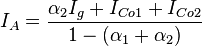

Fig. 5. Energy band diagram in the forward bias mode: equilibrium state, direct locking mode and direct conduction mode.
This equation describes the static characteristic of the device in the voltage range up to the breakdown. After breakdown, the device works as a pin diode. Note that all the terms in the numerator of the right side of the equation are small, therefore, as long as the term α 1 + α 2 <1, the current I A is small. (The coefficients α1 and α2 themselves depend on I A and usually increase with increasing current) If α1 + α2 = 1, then the denominator of the fraction vanishes and direct breakdown occurs (or the thyristor is turned on). It should be noted that if the polarity of the voltage between the anode and cathode is reversed, then the transitions J1 and J3 will be shifted in the opposite direction, and J2 - in the forward direction. Under such conditions, the breakdown does not occur, since only the central transition works as an emitter and the regenerative process becomes impossible. You can also notice that the two-transistor model is used not only to study the processes occurring in the thyristor, but also as its circuit analog in electronic equipment.
The width of the depleted layers and energy band diagrams in equilibrium, in the modes of direct locking and direct conduction, are shown in Fig. 5. In equilibrium, the depletion region of each transition and the contact potential are determined by the impurity distribution profile. When a positive voltage is applied to the anode, the J2 transition tends to move in the opposite direction, and the J1 and J3 transitions in the forward direction. The voltage drop between the anode and the cathode is equal to the algebraic sum of the voltage drops at the transitions: V AK = V 1 + V 2 + V 3 . As the voltage rises, the current through the device increases and, consequently, α1 and α2 increase. Due to the regenerative nature of these processes, the device eventually goes into an open state. After turning on the thyristor, the current flowing through it must be limited by the external resistance of the load; otherwise, at a sufficiently high voltage, the thyristor will fail. In the on state, the J2 junction is biased in the forward direction (Fig. 5, c), and the voltage drop V AK = ( V 1 - | V 2 | + V 3 ) is approximately equal to the sum of the voltage on one straight-shifted junction and the voltage on the saturated transistor.
When the thyristor is in the on state, all three transitions are shifted in the forward direction. Holes are injected from p1, and electrons from n2, and the n1-p2-n2 structure behaves similarly to a saturated transistor with a remote diode contact to n1. Therefore, the device is generally similar to a pin (p + -in + ) -diode ...
When applying a voltage of direct polarity to the anode and cathode of the thyristor with a speed of more than a certain critical dU / dt> dUcrit / dt, the pnpn structure will open. The mechanism of this effect is due to the presence of a parasitic capacitance anode-control electrode. This effect limits the use of thyristors in high-frequency circuits, although it is sometimes used to control a thyristor. The dUcrit / dt parameter is specified in the references for each model of the thyristor.
If the current flowing through the thyristor in the forward direction (in the open state) increases with a speed of more than a certain critical di / dt> diсrit / dt, the structure will be destroyed and the thyristor will fail, due to a limited increase in the carrier flow area, an increase in current density and local thermal breakdown. The parameter dkrit / dt is a reference and is indicated in the catalogs for each model of the thyristor.
By conductivity and the number of conclusions [2] [3] [4] :
Previously, thyristors in the domestic literature were called “controlled diodes”.
Принципиальных различий между динистором и тринистором нет, однако если открытие динистора происходит при достижении между выводами анода и катода определённого напряжения, зависящего от типа данного динистора, то в тринисторе напряжение открытия может быть специально снижено, путём подачи импульса тока определённой длительности и величины на его управляющий электрод при положительной разности потенциалов между анодом и катодом, и конструктивно тринистор отличается только наличием управляющего электрода. Тринисторы являются наиболее распространёнными приборами из «тиристорного» семейства.
Переключение в закрытое состояние обычных тиристоров производят либо снижением тока через тиристор до значения I h , либо изменением полярности напряжения между катодом и анодом.
Запираемые тиристоры, в отличие от обычных тиристоров, под воздействием тока управляющего электрода могут переходить из закрытого состояния в открытое состояние, и наоборот. Чтобы закрыть запираемый тиристор, необходимо через управляющий электрод пропустить ток противоположной полярности, чем полярность, которая вызывала его открытие.

Comments
To leave a comment
Electronics, Microelectronics, Element Base
Terms: Electronics, Microelectronics, Element Base