Lecture
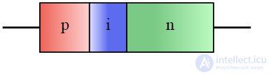
The functional structure of the pin diode
The PIN diode is a kind of diode in which there is an own (undoped, intrinsic) semiconductor ( i -region) between the electron (n) and hole (p) conduction regions. The p and n regions are usually heavily doped, since they are often used for ohmic contact with the metal.
The wide unalloyed i-area makes the pin diode a bad rectifier (a usual use for a diode), but, on the other hand, it allows its use in wattenuators (signal attenuators), fast switches, photodetectors, and also in high-voltage electronics.
Typically designed to work in the centimeter wavelength range.
The characteristic qualities of a pin diode are manifested when operating in the strong injection mode, when the i -region is filled with charge carriers from heavily doped n + and p + areas to which a forward voltage bias is applied. The pin diode can be functionally compared to a bucket of water with a hole on the side: as soon as the bucket is filled to the level of the hole, it begins to leak. Similarly, the diode begins to pass current as soon as it is filled with charge carriers in the i- region.
Due to the fact that in the i-region there is a very low concentration of charge carriers, there are practically no recombination processes during injection. But in the forward bias mode, the concentration of charge carriers by several orders of magnitude exceeds its own concentration.
At low frequencies for the pin diode, the same equations as for the ordinary one are valid. At high frequencies, the pin diode behaves like a near-perfect resistor — its current-voltage characteristic (IVC) is linear even for a very large voltage value. At high frequencies in the i-region there is a large amount of accumulated charge, which allows the diode to work. At low frequencies, the charge in the i-region recombines and the diode turns off.
The reactance is inversely proportional to the direct current flowing through the pin diode. Thus, it is possible to vary the resistance value over a wide range - from 0.1 Ω to 10 kΩ - by changing the DC component of the current.
The large width of the i-region also means that the pin diode has a small capacitance at the reverse bias.
The space charge regions (SCR) in the pin diode are almost completely located in the i- field. Compared to conventional ones, the pin diode has a significantly larger SCR, the boundaries of which vary slightly depending on the applied reverse voltage. Thus, the volume of the semiconductor increases, where electron-hole pairs can be formed under the influence of radiation (for example, optical-photon). Some photodetectors, such as pin photodiodes and phototransistors (in which the base-collector junction is a pin diode), use a pin junction to implement the detection function.
When designing a pin diode, one has to look for a compromise: on the one hand, by increasing the value of the i- field (and accordingly the amount of accumulated charge), the resistive behavior of the diode can be achieved at lower frequencies, but on the other hand, while Closed state will take longer. Therefore, as a rule, pin diodes are each time designed for a specific application.
Pin diodes are typically used as switches in the radio and microwave paths, attenuators, modulators, switches and photo detectors.
By application pin diodes are divided into:
With zero or reverse bias pin-diode has a small capacitance. A small capacitance does not transmit a high frequency signal. With forward bias and a current of 1 mA, a typical pin diode has a reactance of about 1 ohm, which makes it a good conductor in the RF path. Thus, a pin diode can be used as a good RF and microwave switch.
RF relays are also used as switches, but at a lower speed (switching time ~ 10 ms), while pin diodes are much faster: tens of ns, units of microseconds.
The capacity of the switched-off discrete pin diode is approximately 1 pF. At a frequency of 320 MHz, the reactance of such a capacity is ~ 500 Ohm. In systems designed for 50 ohms, the signal attenuation will be about 20 dB, which is not enough in some applications. In applications that require greater isolation, the switches are cascaded: a cascade of three diodes gives attenuation of 60 dB or more (up to 100 dB depending on frequency).
By changing the current through the pin diode, you can quickly change the reactance.
At high frequencies, the pin diode reactance is inversely proportional to the strength of the current. Accordingly, the pin diode can be used as a controlled attenuator, for example, in the schemes of amplitude modulators and level shift.
A pin diode can be used, for example, as a bridge or shunt resistor in a T-bridge attenuator circuit.
Pin diodes are sometimes used to protect devices on inputs during high-frequency measurements. If the input signal is small and is in the range of acceptable values, then the pin diode, as a small capacitor, introduces minimal distortion. When the signal is increased and beyond the permissible limits, the pin diode begins to conduct and becomes a resistor that shunts the signal to ground.
Pin diode can be used in network cards and switches for fiber optic cables. In these applications, a pin diode is used as a photodiode.
As a photodetector, the pin diode operates at reverse bias. However, it is closed and does not pass current (except for a small leakage current). A photon enters the i- region, giving rise to the formation of electron-hole pairs. Carriers of charge, getting into the electric field of the SCR, begin to move to high-alloyed areas, creating an electric current that can be detected by an external circuit. The conductivity of the diode depends on the wavelength, intensity and modulation frequency of the incident radiation.
The magnitude of the reverse voltage can reach large values, with the greater voltage creating a larger field, which pulls the carriers from the SCR of the i -region more quickly.
Some detectors can use the effect of avalanche multiplication of charge carriers.

Comments
To leave a comment
Electronics, Microelectronics, Element Base
Terms: Electronics, Microelectronics, Element Base