Lecture
Electrical circuits of digital and analog equipment are
basic documents in the design, manufacture, commissioning and operation of complex devices. When performing such schemes, along
with the requirements of GOST 2.701-84 and GOST 2.702-75 (see section 1 of the manual), a number of specific requirements established by GOST 2.708-81 should be taken into account. The rules established by these standards provide for manual or automated documentation. To cover the most common conventional graphic symbols (HBL) of elements of digital and analog equipment - the main goal of Sec. 3 textbooks.
UGO elements of digital technology (CG) are based on a rectangle (GOST 2.743-82). In general, a HBM may contain a main field and one or two additional fields located on either side of the main field (Fig. 3.1). Consequently, the size of the HBP depends on:
The width of the main field must be at least 10 mm, additional - at least 5 mm, the distance between the terminals - at least 5 mm, the distance between the output and the horizontal side (or the boundary of the zone) of the UGO - at least 2.5 mm or a multiple thereof. It is allowed to increase the width of the fields when applying a large number of labels and functions. Conclusions can be combined into groups that are separated by an interval of at least 10 mm or a multiple of 5 mm.
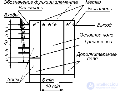
Fig. 3.1. Recommended dimensions and designations of the element of the CG
The conclusions of the elements are divided into inputs, outputs, bidirectional conclusions and non-informational. The inputs are on the left and the outputs are on the right. Allowed rotation of the UGO 90 ° clockwise (Fig. 3.2).

Fig. 3.2. Arrangement of conclusions and designations at turn of the element of TsT
The functional purpose of the element of digital technology is indicated in the upper part of the main field of the UGO (Fig. 3.1), which consists of capital letters of the Latin alphabet, Arabic numerals, special signs and symbols, entered without spaces. The designation of the main functions and their derivatives are summarized in Table. 3.1.
Table 3.1
Designation of the main functions of DH and their derivatives
|
Main function |
Code functions |
|
Calculator computing device (CPU) CPU Processor section Memory Random Access Memory random access sequential access Permanent memory with disposable and reusable programming Control Transfer Interrupt Broadcast Reception Serial I / O Parallel input / output Arithmetic Summation Subtraction Multiplication Division Logics Logical and Logical or Exclusive or Repeater Register Shift register from left to right Register with shift from right to left Reverse Shift Register Counter binary decimal Decoder Encoder Converter Comparison Multiplexer Demultiplexer Multiplexer selector |
CP
CPU P PS M
Ram SAM
Prom Rprom CO CR INR Tf RC Ios IOP A SM SUB MPL Div L & or and ³1 = 1 one Rg RG® Rg¬ RG " CT CT10 DC CD X / y = = Mux DMX MS |
The end of the table. 3.1
|
Main function |
Code functions |
|
Selector Generator continuous pulse train single pulse (one-shot) sine wave signal Trigger two-stage Schmitt Shaper logical 0 logical 1 Key Modulator Demodulator Non logical elements Stabilizer stresses current Sets (assemblies): resistors diodes transistors indicators |
SL G GN G1 GSIN T TT TH F FL0 FL1 SW MD DM * ST STU STI
* R * D * T * H |
In some elements of the CG, double designation is allowed. For example, in the designation of one-shot, except for the alphanumeric code G1, listed in Table. 3.1, you can use a symbol in the form of a rectangular pulse of positive polarity (P), in the designation of triggers - a symbol similar to a hysteresis loop. Non-logical elements of the CT - sets of resistors, diode and transistor arrays, etc., are marked with an asterisk (*). If necessary, this designation complement the technical characteristics. A resistor assembly, for example, may be designated as * R150-8, i.e., eight resistors with a resistance of 150 ohms each.
The complex functions of the CG element are shown by a combination of simple ones. For example, a binary counter with a decoder is indicated by the combination CT2DC, write control ( WR ) - COWR , decoder ( DC ) interrupts ( INR ) - DCINR , etc.
Recently, more and more often we have to deal with foreign digital and analog equipment. It should be noted that in UGO of its elements, the ESKD standards are closest to the standards of the EEC countries, in particular, BS3939 (United Kingdom) and are very different from the USSI standard. Conventions of the listed functional schemes see in subsection. 3.2.
Conclusions of the elements of the CG distinguish between static and dynamic.
In turn, each of them can be direct or inverse.
These provisions are reflected in the UGO (Fig. 3.3). Direct static outputs are represented by lines connected to the main or additional fields, without additional symbols (Fig. 3.3, a ).
Direct inverse pins are marked with a circle at the point of attachment with fields (Fig. 3.3, b , c , d , e ). The preferred designations are in Fig. 3.3, b , c ).
Symbols such as slashes, arrows, and triangles are used to denote dynamic inferences. In fig. 3.3, e , g , and the notation for direct dynamic conclusions are shown, and in fig. 3.3, k , l , m , n - inverse dynamic conclusions. The designations shown in fig. 3.3, e , g , k , l .
Non-informational output is marked with a cross, which is applied at the point of its connection with the field or near the field (Fig. 3.3, p , p , c ). If the non-informational conclusions are grouped, then the symbol is placed in a zone on a line in common with the main field (Fig. 3.3, c ).
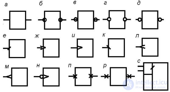
Fig. 3.3. Marking of the findings of the element DH
Pin assignments are indicated by labels in additional fields. Tags are a combination of Latin letters, Arabic numerals and special characters. The designation of the main labels are given in table. 3.2.
Table 3.2
Pin Assignment and Encoding
|
Destination output |
Code tags |
|
Set to n one 0 initial state (reset) Allow installation of universal JK-trigger in the state one 0 Input increase the content of the element by n Reduction input element content by n Address Coordinate addressing X Y More More or equal Equality Less Less or equal Bit Byte Conditional bit - “flag” Lock (ban) Buffer Readiness Data Loan Record Reading Request Capture Execution (end) Instruction (command) Control Marker Start |
Sn S R SR
J K + n -n "Or <> A
X Y > ³ = < £ Bit BY EL DE Bf RA D BR Wr RD Rq TR END INS CH MR Bg |
The end of the table. 3.2
|
Destination output |
Code tags |
|
Expectation Answer Transfer Spreading Transfer generation Overflow Replay Continuation A priority Start Resolution Expansion Regeneration Synchronization Strobe, tact Younger Average Older Tire Inversion
|
WI AN CR CRP CPG Of RP CN PR ST E EX Ref SYN C LSB ML MSB B IN
|
To designate the so-called open conclusions of the elements of the CG, special symbols are used, such as a diamond (Fig. 3.4, a ), a circle with four rays (Fig. 3.4, b ).
If it is necessary to clarify that this pin is connected to the collector of the transistor of the p – n – p structure, the emitter of the transistor of the n – p – n structure, the drain of the field-effect transistor with the p-channel or the source of the field-effect transistor with n-channel, the diamond is provided with a dash from above (Fig. 3.4, c )
and the circle — the corner with the “opening” facing him (Fig. 3.4, d ).
If the listed electrodes belong to transistors of the opposite structure or field-effect transistors with channels of the opposite type, then the dash at the diamond is located below
(Fig. 3.4, d ), and the top of the corner is directed towards the circle (Fig. 3.4, e ).
Conclusions that have a high impedance state (Z-state) are denoted by a diamond with a dash inside (Fig. 3.4, g ) or the Latin letter Z (Fig. 3.4, и ).
Labels of complex functions of the conclusions are simple. For example, to specify the resolution (E) of the record (WR), use a combination of EWR, and the resolution of reading - reading (RD) - ERD, etc. As labels of conclusions it is allowed to use the notation of functions and their derivatives from Table. 3.1.
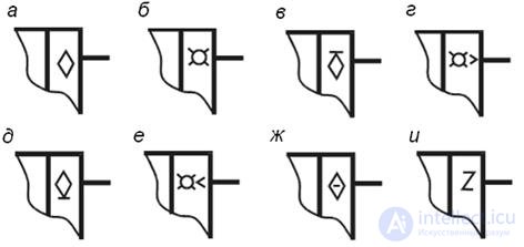
Fig. 3.4. Marking the findings of the element of the CG with the specification of the structure of the device
For the numbering of digits in groups of pins, digits corresponding to their numbers are added to the label designations. For example, informational output of the zero digit is denoted D0, the first is D1, and the second is D2, etc. The zero digit is denoted as D1, the first is D2, and so on.
To reduce the number of characters in the label, it is allowed to indicate the degree of its base instead of the weighting factor. For example, an information input with a weighting factor of 256 (2 8 ) can be designated D8 or 8, where the arrow explains that the number indicates the degree.
If the conclusions are equivalent and their functions are uniquely determined by the function of the element, then the CSB does not contain additional fields. In this case, the distances between the terminals are equal, and the side of the HBO, to which the terminals are adjacent, is also divided into equal parts. For example, a two-input element 2И-НЕ will divide the side of the HBM into three equal parts (Fig. 3.5, a ). Label logic conclusions located in the UGO opposite the first input from the top. It is allowed to combine equivalent logical conclusions into a group with assignment of a label in an additional field. So, for example, the “&” label means that all five outputs of the element are combined by a logical function AND, and the letter R indicates that each output (Fig. 3.5, b ) serves to set the logical element to the state 0. Other labels and letters are selected by purpose (table 3.2). It is allowed to combine the labels of the output of an element into a group if a unique function is performed (Fig. 3.5, c , d ).
Bidirectional leads are labeled with a double-headed arrow or two “<>“ signs. It is customary to place similar labels above the label of the input function and under the label of the output function, as shown in Fig. 3.6, in designation of the input function XA and the output function YА.

Fig. 3.5. Pin marking with labels
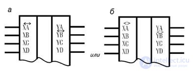
Fig. 3.6. Bidirectional pin marking
If the output has several functional purposes and / or interconnections, then they are also grouped together, recording labels one under the other (Fig. 3.7, a ). At specification of performance of this or that function and / or interrelations apply the symbols shown in fig. 3.7, b. In this example, with a signal equal to logical 1, the X1 function is performed, with a logical 0 - the X2 function, when the signal passes from level 0 to 1, the X3 function is performed, and vice versa - the X4 function.
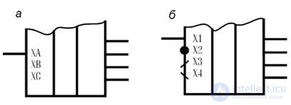
Fig. 3.7. Designation of conclusions having several logical functions
For pins that do not carry logical information (these include power pins, electrodes of semiconductor devices, pins for connecting resistors, capacitors, quartz resonators in frequency-setting circuits), use alphanumeric code labels. For example, in fig. 3.8, and shows a fragment of the UGO chip in which the outputs of bipolar power sources are indicated in one field, the output of a collector p-n – p collector and the emitter output E of the n – p – n transistor in another field. The third field contains pins for connecting a resistor, a capacitor, an inductor and a quartz resonator.
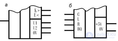
Fig. 3.8. Designation of conclusions without logical functions
This tutorial does not provide typical UGO of digital circuit elements based on AND, AND-NOT, OR-NOT, AND / OR-NOT logic, trigger devices, counters, registers, decoders and encoders, multiplexers, etc. You can find them in reference books on digital integrated circuits [4].
Let us dwell on some of the techniques used when drawing diagrams of digital devices.
For example, rice. 3.9 explains that if a device contains several identical elements with the number of terminals of the same functional value, then one of these elements is allowed to be drawn in full, and the others are simplified.
Fig. 3.9. Simplification when repeating the same elements
Since digital integrated circuits can contain several identical logical or other elements in one building, it is allowed to depict their schemes in a combined and spaced manner (Fig. 3.10).
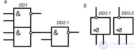
Fig. 3.10. UGO identical elements IC
Identical elements forming a column or row may be separated by electric communication lines (Fig. 3.11).
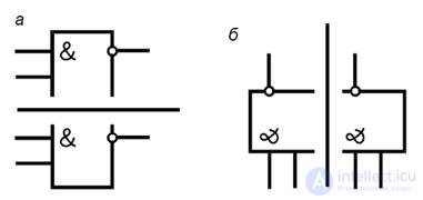
Fig. 3.11. Separation of elements by electric communication lines
In this case, the contour lines of the UGO are drawn not completely, but with a gap of at least 1 mm to the electric communication line.
Elements of analog technology include various amplifiers.
(including summing, differentiating, integrating, etc.), functional, analog-digital and digital-analog converters (ADC and DAC), electronic switches, switches, etc. Most often, these devices are manufactured in the form of integrated circuits, therefore in the positional notation on the diagram apply the code DA.
UGO elements of analogue equipment set GOST 2.743-82 and GOST 2.759-82.
The UHD products of this group are constructed in the same way as the symbols of the elements of digital technology. This means that in addition to the main field, they may contain additional fields, and their number and size are determined by the number of pins, the number of characters in the labels, the notation for functions, etc.
The inputs of the elements of analogue equipment are placed on the left, and the outputs are located on the right of the UGO. The image can be rotated 90 ° clockwise. In this case, the input element will be located at the bottom, and the output - at the top. Inverse input, in contrast to direct, is indicated by a circle at the point of attachment to the contour of the HGO element (Fig. 3.12).
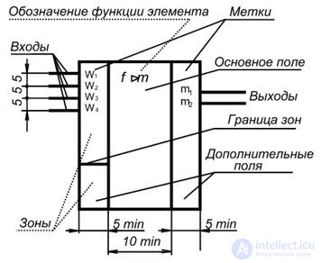
Fig. 3.12. Recommended dimensions and designations of the element of analog technology
Externally, the UGO analogue technology is almost the same as digital (compare Fig. 3.1 and 3.12). The difference lies in the functional designation of elements. The designations of the most common functions in the analog technique are shown in Table. 3.3.
Table 3.3
The designation of functions in analog technology
|
Function name |
Code |
|
Detection |
Dk |
|
Division |
X: Y or x: y |
|
Frequency division |
: FR or: fr |
|
Differentiation |
D / DT or: d / dt |
|
Integration |
Int or: ò |
|
Logarithm |
LOG or: log |
|
Short circuit |
SWM |
|
Breaking |
SWB |
|
Switching |
SWT |
|
Transformation |
X / Y or x / y |
|
Analog-to-digital conversion |
Ù / # |
|
Digital to Analog Conversion |
# / Ù |
|
Comparison |
= = |
|
Summation |
SM or S |
|
Trigonometric functions: sine cosine tangent cotangent |
Sin or sin Cos or cos Tg or tg CT or ct |
|
Multiplication |
Xy or xy |
|
Gain |
> or |
Symbols of complex functions, as in digital technology, are simple. It is allowed to use in case of need the designations established for digital equipment (tab. 3.1 and 3.2).
Pin assignments are indicated by tags that are placed in additional fields. The designations of the main labels are given in table. 3.4.
Table 3.4
Tagging Analog Technology
|
Output label |
Code |
|
Balancing (correction 0) |
NC |
|
Frequency correction |
FC |
|
Initial value of integration |
one |
|
General conclusion |
0V |
|
Maintain current signal value |
H |
|
Nutrition: from voltage source (general designation) from voltage source (e.g. +15 V) |
U
+ 15 V |
|
Start |
ST |
|
Strobe, tact |
C |
|
Setting the initial value |
S |
|
Set to 0 |
R |
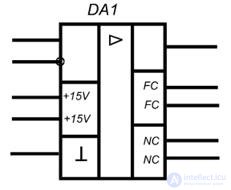
Fig. 3.13. UGO operational amplifier
UGO of the operational amplifier is shown in fig. 3.13. It has one output (top right in the figure) and two inputs: direct (non-inverting), since the output signal phase coincides with the phase of the signal applied to the input) and inverse (inverting) - the output signal phase is shifted by 180 ° relative to the signal received at the entrance. The pins labeled “+ 15V” and “–15V” are designed to connect a bipolar ± 15V power supply. The pins labeled FC are designed to connect an external circuit, correcting the frequency response of the operational amplifier. Note that some types of operational amplifiers have internal frequency response correction circuits. The NC (zero correction) terminals are connected to the elements of the zero voltage setting at the output in the absence of a signal at the inputs. If the operational amplifier is made in a metal case and has an output, the latter is designated as an inverted T. This output should not be confused with the output of a common bipolar power wire, which is assigned a 0V mark.
Examples of UHD elements of analog technology are summarized in Table. 3.5.
Table 3.5
Примеры УГО элементов аналоговой техники
по ГОСТ 2.759-82
|
Наименование и выполняемая |
УГО элемента |
|
Усилитель инвертирующий (инвентор) с коэффициентом усиления 1 u = – 1a |
|
|
Усилитель суммирующий u = –50(0,1 + 0,2b + 0,4c + 0,8d) |
|
|
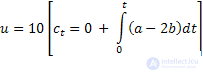
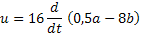
Усилитель интегрирующий
Если f = 1; g = 0; h = 0, то
|
|
|
Усилитель дифференцирующий
|
|
Окончание табл. 3.5
|
Наименование и выполняемая |
УГО элемента |
|
Перемножитель с коэффициентом передачи u = – Kab |
|
|
Divider
|
|
|
Усилитель логарифмирующий u = log(a – 2b) |
|
|
Преобразователь сигналов , общееобозначение |
|
|
Преобразователь полярных координат в прямоугольные u 1 = a cos b u 2 = a sin b |
|
1. На какие поля делится УГО элемента цифровой техники?
2. От каких параметров зависят размеры элемента УГО?
3. Как маркируется инверсный вывод элемента цифровой техники?
4. What is the letter designation of the UGO element of digital technology?
5. What symbol denotes the bidirectional output element of the UGO digital technology?
6. What are the simplifications of the UGO when repeating the same elements?
7. What is the letter code HGO element analog equipment.
8. What is the difference between UHD elements of analog and digital technology?


Comments
To leave a comment
Electronics, Microelectronics, Element Base
Terms: Electronics, Microelectronics, Element Base