It is necessary to distinguish the noise figure of the input device itself and the noise figure of the input device and the first receiver stage, which are determined jointly. We first consider the latter case as more general, and then as a particular case, we determine the noise factor of the input device itself.
The noise ratio of the input circuit taking into account the first cascade of the receiver.
When calculating the noise figure, the antenna noise as a signal source, the noise of the input device itself and the noise of the first stage, counted at its input, are taken into account.
Suppose that the conductance of the signal source recalculated to the input of the first stage is
 ,
,
and its own noises are characterized by noise current.
 .
.
Conductivity of the resonant circuit
 ,
,
counted to the input of the first cascade, causes the appearance of noise current
 .
.
The noise of an electronic device standing at the entrance is recalculated to its input and is characterized by the source of the noise.
 ,
,
Where  - noise resistance.
Obviously, it is also necessary to take into account the noise that appears in the input conductivity of the electronic device, and these noises are represented by noise current.
 ,
,
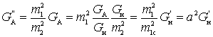
Where  - relative noise temperature of noise, which shows how many times the noise of the real input conductance is greater than the noise of the corresponding ohmic resistance.
Values and  is given in reference books or calculated using formulas known from the course of electronic devices. The value of P represents the effective noise bandwidth of the receiver. Given the above about the sources of noise, the equivalent noise scheme can be represented as follows.
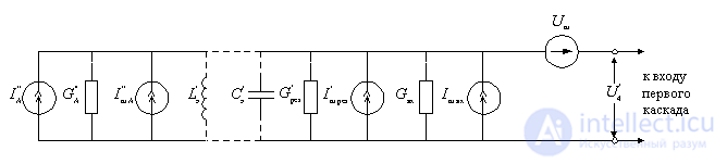
Figure 6.6.
As can be seen in the conductivity figure  ,
,  ,
,  are respectively sources of noise
  ,
,  ,
,  and the amplification device - the source of noise
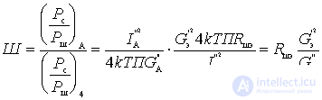
The noise figure of the system, in accordance with the definition, can be represented as a ratio of signal power and noise in the antenna and at the output of the circuit, i.e.
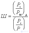 .
.
The signal-to-noise ratio in the antenna as the source is determined by its data. In particular, the nominal power of the antenna as a signal source and noise source
 ;
;  .
.
Their attitude is
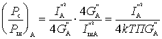 .
.
We now find the signal-to-noise ratio at the output.
The nominal signal power and output noise are respectively
 ;
;  ,
,
Where
 .
.
- the resulting conductivity of noisy sources.
Find the noise voltage at the terminals 4-4 "
 ,
,
Where

or
 .
.
Considering the values  ,
,  ,
,  the total noise voltage at the output of the circuit
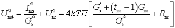 .
.
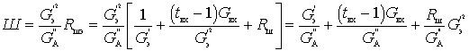
The expression in square brackets is the resulting noise resistance of the input device and the first cascade:
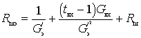 .
.
Three members of this sum characterize the noise properties of the following sources:
a) the input device itself, whose noise properties are determined by the resistance recalculated to the input of the first stage, i.e. by size
 .
.
b) the input of the first stage, the noise properties of which are determined by additional noise in the input resistance of the electronic device
 ;
;
c) an amplifier device, whose noise properties are determined by noise resistance  .
.
We now determine the signal-to-noise ratio at the output of the circuit.
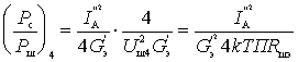 .
.
Then the noise figure
 .
.
Providing the required modes when choosing the connection between the antenna, the loop and the input of the first stage.
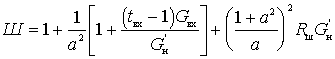
Let us consider in more detail the expression for the noise figure, substituting in it the value of the resulting noise resistance:
 .
.
Taking into account that
 .
.
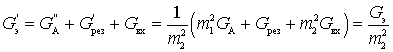
Where  - recalculated to the input of the first cascade load conductance.
 .
.
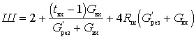
Noise figure can be written
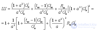 .
.
The second term characterizes the additional value of W due to the circuit noise and the input of the first cascade.
The third term characterizes the additional value W at the expense of an electronic device.
Analyzing the last expression, we consider 3 particular cases of choosing the connection between the antenna, the input circuit and the input of the first cascade:
but) the first particular case is the power matching mode , in which the matching is performed at the receiver input, i.e. transformation ratio (inclusion)  is taken equal to the matching value
  Because in negotiation mode
  then the noise figure is determined
 .
.
In the region of relatively high frequencies, when
 ,
,  ,
,
noise figure
 ,
,
those. determined by the values  and
and  . From this it follows that in order to reduce the noise figure, it is necessary to choose electronic devices with the lowest possible values. and
  .
.
b) The second special case is the noise matching mode .
This case is characterized by the fact that the inclusion coefficient from the antenna , as in the previous case, is taken equal to the matching value, i.e.  and mismatch factor .
At the same time, the contour is connected to the input of the first cascade not arbitrarily, but in a quite definite way, by choosing some optimal value of the switching coefficient.  in order to reduce the noise figure.
The expression for the noise figure given that 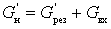 take the form
 ,
,
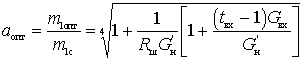
In order to find the optimal value of the coefficient of inclusion in terms of noise figure  take the derivative
  by
by  and equate it to zero.
From here
 .
.
Then
 ,
,
those. noise factor is determined only by the parameters of the electronic device.
A decrease in the noise figure due to incomplete connection of the circuit to the input of the first cascade is due to the action of two factors: a decrease in the recalculated value of the resonant resistance of the circuit  , resulting in a sharp decrease in noise level (in proportion to
  ), and at the same time reducing the level of the useful signal removed from the contour
  (proportionally ).
at) the third special case is the mode of optimal noise mismatch .
In this case, the coefficient from the side of the antenna is not taken equal to the matching value, but its optimal value is found  (or
(or  ), at which the noise figure gets the minimum value
  .
.
For determining we write W in the form
 .
.
Take the derivative of this expression for a  , we equate it to zero and find
 .
.
Then
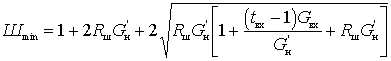 .
.
In the region of relatively high frequencies, when  , size
  and
and
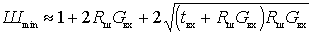 .
.
those. noise factor is determined only by the parameters of the electronic device.
Decrease in noise figure at  is achieved by reducing the influence of the noise of the resonant circuit and the cascade input.
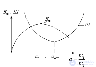
Figure 6.7.
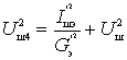
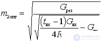
The noise figure of the input device without taking into account the influence of the first cascade.
As already shown
 ;
;  .
.
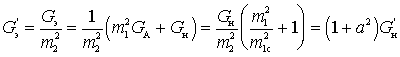
For the input device without taking into account the influence of the first cascade
 ,
,
 .
.
Attitude
 .
.

Comments
To leave a comment
Devices for the reception and processing of radio signals, Transmission, reception and processing of signals
Terms: Devices for the reception and processing of radio signals, Transmission, reception and processing of signals