Lecture
The input filter is one of the most important nodes of the receiving device. As was shown in previous chapters, in communication systems with a large ratio of the upper operating frequency to the lower operating frequency, this filter must be tuned in frequency. Frequency tuning can be done in LC filters. The more complex the filter will be used as an input filter, the higher the quality of the receiving device will be obtained, however, there are problems with a simultaneous change in the frequency of setting the circuits, changing their quality factor and providing the necessary depth of communication between these circuits.
Most often, a system of two coupled loops is used as a bandpass tunable filter. In the most important schemes put a three-loop filter. In this case, it is possible to obtain a sufficiently steep slope of the amplitude-frequency characteristic. In some cases, asymmetrical slope of the frequency response is used (see Figure 7).
The use of both sequential and parallel oscillatory circuits allows you to implement different values of input and output resistances. Such a filter allows, in addition to attenuating disturbing signals, to coordinate the resistances of the signal source and the load. Such a filter is called L-shaped. The classical scheme of the L-shaped bandpass filter is shown in Figure 1.
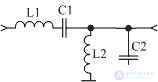
Figure 1 L-Band Filter Diagram
This filter uses a serial L1C1 circuit and a parallel L2C2 circuit. The input and output impedance of the filter in general can be different. This can be useful when designing a duplexer, but most often the input and output impedances are made equal to 50 Ohms. This choice allows the use of standard measuring instruments for tuning the receiver. The calculation of the l-shaped bandpass filter is quite simple. First, the equivalent Q factor of the filter contours is determined.
 (one)
(one)
where f 0 is the average frequency of the range;
 - filter bandwidth.
The values of the reactive elements of the L-shaped bandpass filter shown in Figure 1 can be determined by the following formulas:
 ,
,  ,
,  ,
, 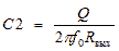 . (2)
. (2)
The selectivity of one L-shaped link of the filter may not be enough, then the two links can be connected in series. You can connect them either by parallel branches to each other (this results in a T-shaped bandpass filter), or sequential ones (in this case, a U-shaped bandpass filter is obtained). The elements L and C of the connected branches are combined.
As an example, Figure 2 shows the scheme of a U-shaped bandpass filter. The L2C2 elements remained the same, and the elements of the serial circuits combined into the inductance L = 2 · L and the capacitance C = 0.5 · C 1. At the same time, since the product LC remained the same, the tuning frequency of the serial circuit remained the same and equal to the average frequency of the filter .
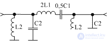
Figure 2 Diagram of the U-shaped bandpass filter
It should be noted that the above is a simplified version of the calculation of the input filter. Much better results are given by standard methods of calculating filters with approximation of the amplitude-frequency characteristic according to Chebyshev or Butterworth. With the same number of reactive elements, the filter can provide a greater steepness of the slopes of the amplitude-frequency characteristic.
In radio-frequency filters, it is convenient to use only parallel oscillatory circuits. Such a filter requires a few more elements to implement the same frequency response. The scheme of a double-circuit bandpass filter with an external capacitive coupling is shown in Figure 3. The inductance and capacitance of the circuits are calculated by formulas (1) for L 2 and C 2, and the capacitance of the coupling capacitor can be determined by the formula C 3 = C 2 / Q.
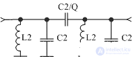
Figure 3 Scheme 2-bandpass bandpass filter
To increase the selectivity in the image channel, you can turn on three or more identical circuits, reducing the capacitances of the C3 coupling capacitors by 1.4 times. A similar scheme of a 3-loop bandpass filter is shown in Figure 4.
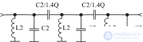
Figure 4 Scheme 3-bandpass bandpass filter
As already discussed when developing a block diagram of a radio receiver, the narrower the passband of the receiver input filter, the better. Therefore, the input filters of receivers are often made tunable in frequency. Typically, the adjustment of the filter circuits in frequency is carried out using variable capacitance. This allows you to increase the quality factor of the circuit with an increase in the frequency of tuning the circuit and, thereby, maintaining the same filter bandwidth when tuning in frequency.
In order to make sure that the bandwidth of a single circuit is kept constant during frequency tuning using capacitance, we turn to the formula for determining the quality factor:
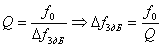
Now we express the quality factor through the relation of the reactive and active resistance of the circuit:

where the reactance of the circuit is defined as follows:

As a result, it can be concluded that the quality factor of the circuit, with an increase in its tuning frequency by decreasing the capacitance of the capacitor, will increase in proportion to the root of the capacitance.
The formula for the frequency of tuning the circuit depends on the change in capacitance in a similar way:

and, therefore, the ratio of the frequency of tuning the circuit and the quality factor, which determines its bandwidth, will be constant.
As the variable capacity is most convenient to use varicap. One of the variants of the circuit diagram of the input tunable filter is shown in Figure 5.
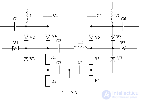
Figure 5 Schematic diagram of the receiver input filter
In this scheme, a U-shaped bandpass filter is implemented, the scheme of which is shown in Figure 2. In the scheme shown in Figure 5, the input parallel circuit is formed by elements L1, C1, V1, V3, the output parallel circuit is formed by elements L3, C5, V7, V8 . The serial loop in this circuit is implemented by the elements L2, C2, V2, V4, V5, V6. Capacitors C1 and C6 are decoupling capacitors.
In mobile communication systems operating in the VHF band, the ratio of the upper operating frequency to the lower operating frequency does not exceed 1.2, therefore, the tuning coefficient determined by the varicaps has to be reduced with additional capacitors C1, C2, C5.
The configuration of the circuits in this scheme is carried out by applying a control voltage through resistors R1, ..., R4. Capacitors C3 and C4 are designed to suppress interference and interference in the control circuit.
In cellular communication systems, the ratio of the upper operating frequency to the lower operating frequency does not exceed 1.04, i.e., the width of the entire operating frequency range is only 4% of the average frequency of the range. This allows you to abandon the adjustment of the input filter in frequency and perform the filter in the form of a band-pass filter with constant parameters. To minimize the size of the filter, it is possible to make a surfactant technology or to implement a ceramic filter.
As an example of such a filter, figure 6 shows the appearance of the smd receiving filter SAFEA942MFL0F00 of the company Murata, made on surface acoustic waves.
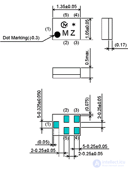
Figure 6 The appearance of the receiving filter
The amplitude-frequency characteristic of the SAFEA942MFL0F00 filter from Murata, performed on surface acoustic waves, is shown in Figure 3. This filter is designed to work as an input filter of a mobile device receiver in the GSM900 communication system.
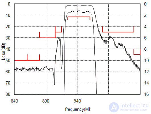
Figure 7 The frequency response of the input filter of the receiver GSM900

Comments
To leave a comment
Devices for the reception and processing of radio signals, Transmission, reception and processing of signals
Terms: Devices for the reception and processing of radio signals, Transmission, reception and processing of signals