Lecture
A large and constructively deficient OU is the presence of an initial displacement at their input. This offset can be disregarded when constructing AC amplifiers based on an op-amp, since they usually use split capacitors. When constructing DC amplifiers, it is necessary to reckon with the need to compensate for the constant bias at the input of an opamp. This voltage is not stable and may change with changes in temperature, operation time and for other reasons.
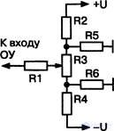
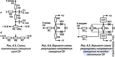
Fig. 4.2. Variant of the initial offset compensation scheme
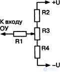
Fig. 4.7. Compensation scheme of the initial offset at the input of the OS
Some circuit solutions designed to solve the problem of compensating the initial bias at the input (s) of the OS are given below. The simplest scheme (Fig. 4.1) consists of a regulating potentiometer R3. Resistor R1 is designed to reduce the influence of the regulating element - potentiometer R3 on the input resistance of the amplifier. Resistors R2 and R4 provide a "stretch" of the control range, a smoother and more accurate adjustment.
Indicative values of the circuit elements: potentiometer R3 - ed .... hundreds of kilo-ohms, R1 - two orders of magnitude or more above the values of resistors connected to the input of an op-amp; R2 = R4 - an order of magnitude higher than the nominal value of R3.
The variant of the initial bias compensation scheme based on resistive dividers (Fig. 4.2) allows for a smooth adjustment of the voltage. To implement the scheme, usually R2 = R4 "(R3" R5 = R6). For example, R2 = R4 = 33 kΩ; R3 = 200 Ohm; R5 = R6 = 27 Ω, Rl = 10 kΩ. This allows you to adjust the bias voltage within ± 10 mV at typical power supply voltages OU ± 12.6 V.
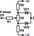
Fig. 4.6. Bias Voltage Adjustment Option
OU zero offset compensator, fig. 4.3 (top), allows you to smoothly adjust the voltage at the input of the operational amplifier in the range from +150 to -150 mV. Narrow the limits by 3 times by increasing the value of the resistor R3 to 3 MΩ, or by reducing the value of the resistor R2 to 3.0-3.3 kΩ. The third option is to replace the potentiometer R6 with a chain of equal resistance R5 = R6 = R7, fig. 4.3 (bottom).
Another variant of the compensation scheme for the initial displacement of an op amp, fig. 4.4, uses to stabilize the bias voltage two forward-bias diode VD1 and VD2. The development of this idea is the following scheme, Fig. 4.5. To further improve the stability of the bias voltage, stable current generators (GTS) U are used as which, in the simplest case, high-resistance resistors can be used.
Simple GTS are also considered in the book [4.1, 4.2]. Scheme, Fig. 4.5, due to the parallel connection of several regulating elements R2j — R2 n, it is possible to compensate, independently of each other, the initial bias voltages of several OU
I note that not only semiconductor germanium or silicon diodes or their successively connected chains, but also special elements designed to stabilize the voltage - stabistors, zener diodes, specialized microcircuits, fig. 4.6.
Other methods of compensation are described in more detail in the monograph [4.3].
Shustov M. A., Circuitry. 500 devices on analog chips. - SPb .: Science and Technology, 2013. —352 p.

Comments
To leave a comment
Electrical Engineering, Circuit design
Terms: Electrical Engineering, Circuit design