Lecture
The characteristics of electronic devices are largely determined by the mode of operation of the transistor. However, the mode of operation of the transistor depends on many factors and primarily on the gain of the transistor itself. The gain of the transistor varies depending on the temperature, the variation of the parameters of the transistors themselves, the supply voltage, and radiation.
The emitter stabilization circuit has the best parameters, however, in some cases, the collector stabilization is sufficient to stabilize the transistor cascade mode. Especially it can be said about the schemes of radio frequency amplifiers and intermediate frequency amplifiers. A diagram of the collector stabilization in a cascade with a common emitter is shown in Figure 1.
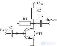
Figure 1. Diagram of the collector stabilization in a cascade with a common emitter
A diagram of the collector stabilization in a cascade with a common collector is shown in Figure 2.
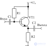
Figure 2. Diagram of the collector stabilization in a cascade with a common collector
In this circuit, the resistor from the collector circuit is moved to the emitter circuit. From the point of view of the physics of the collector stabilization work, this does not matter. Similarly, the collector stabilization circuit in a cascade with a common base also looks like. Similarly, the collector stabilization circuit in a cascade with a common base also looks like. A diagram of the collector stabilization in a cascade with a common base is shown in Figure 3.
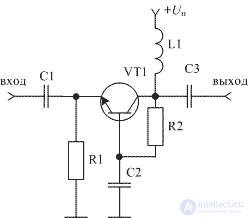
Figure 3. Diagram of the collector stabilization in a cascade with a common base
In this scheme, the L1 choke is used as a cascade load for alternating current. It does not have direct current resistance, therefore the collector stabilization circuit shown in Figure 3 does not differ from the circuit shown in Figure 2. As a variant of this circuit, the resistance R1 and the choke L1 can be swapped. In this case, the resistor R1 will be the load of the cascade, and the choke L1 will provide the DC path.
All the DC circuits are equivalent. A generalized diagram of the collector stabilization (DC switching circuit) is shown in Figure 4.
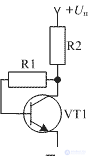
Figure 4. Generalized collector stabilization scheme
Consider the work of the collector stabilization. Let the collector current increase due to destabilizing factors (the temperature of the transistor increased, the supply voltage increased, or a transistor with a high current gain h21E was used in the circuit). According to Ohm’s law, the voltage drop across resistor R2 will increase, and since the voltage at the collector is:
U p = U to + U R2, therefore U to = U p - U R2
then the voltage at the collector will decrease. This will reduce the voltage at the base of the transistor, which will cause a decrease in the base current. Since the collector current can be determined from the expression
i k = i b × h 21e
then the collector current will also decrease and return to the original value. The considered chain of reasoning proves that the collector stabilization ensures the stability of the transistor cascade.
Now compare the efficiency of the emitter and collector stabilization. In the emitter stabilization circuit, the entire voltage drop across the emitter resistance is applied to the base transition. In the collector stabilization scheme, the voltage at the collector decreases to the voltage U BE. In this circuit, there is a voltage divider formed by the resistances R1 and Rin. It reduces the depth of negative feedback, and hence the effectiveness of stabilization.
Now consider how you can calculate the value of the elements of the collector stabilization scheme. The voltage on the collector of the transistor to obtain the maximum dynamic range is chosen equal to half the power of the circuit. The collector current is chosen at which the maximum gain of the transistor will be (according to the directory). Usually it is 1 ... 5 mA. According to Ohm's law, the resistance of the resistor R2 will be equal to:
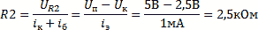
Resistor R1 is calculated almost the same way as in the circuit with a fixed base current. First, determine the base current:
i b = i k / h 21 e = 1 mA / 20 = 50 μA
Then again use Ohm’s law:
R 1 = ( U c - U b) / i b = (2.5 V - 0.7 V) / 50 μA = 36 kΩ

Comments
To leave a comment
Electrical Engineering, Circuit design
Terms: Electrical Engineering, Circuit design