Lecture
The characteristics of electronic devices are largely determined by the mode of operation of the transistor. However, the mode of operation of the transistor depends on many factors and primarily on the gain of the transistor itself. The gain of the transistor over the current h21e varies with the temperature, the variation of the parameters of the transistors themselves, the supply voltage, and radiation.
To stabilize the operation mode of the transistor, negative DC feedback is used, and the emitter stabilization circuit has the best characteristics. In radio frequency amplifier and intermediate frequency amplifier circuits, emitter stabilization is used as often as in low-frequency amplifier circuits. The scheme of emitter stabilization in a cascade with a common emitter is shown in Figure 1.
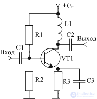
Figure 1. Emitter stabilization scheme in a cascade with a common emitter
Note that the circuit is for a bandpass amplifier, such as an intermediate frequency amplifier or a radio frequency amplifier. The scheme of emitter stabilization in a cascade with a common collector is shown in Figure 2.

Figure 2. Emitter stabilization circuit in a cascade with a common collector
Similarly, the emitter stabilization scheme in a cascade with a common base also looks like. The scheme of emitter stabilization in a cascade with a common base is shown in Figure 3.
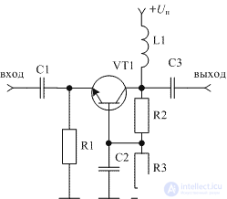
Figure 3. Emitter stabilization scheme in a common base cascade
As can be seen from Figures 1 ... 3, the emitter stabilization scheme in cascades with different switching on of the transistor does not change. Only the input and load connections are changed. Therefore, the operation of the emitter stabilization circuit can be considered without taking into account the transistor AC switching circuit. A generalized emitter stabilization circuit (DC switching circuit) is shown in Figure 4.
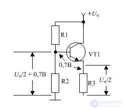
Figure 4. Generalized emitter stabilization scheme
Consider how this scheme works. In the emitter stabilization circuit, the current through resistors R1 and R2 is set several times greater than the base current of the transistor. As a result, the voltage at the base of the transistor does not depend on its base current. Let the collector current of the transistor increase by increasing the temperature or the supply voltage. Then, by Ohm's law, the voltage drop across the resistor R3 will increase. The voltage at the emitter of the transistor increased. But the voltage at the base of the transistor is equal to the sum of the voltage at the emitter and the voltage of the base-emitter of the transistor:
U b = U e + U be
So the base-emitter voltage of the transistor is equal to:
U be = U b - U e
If the voltage at the emitter increases, the voltage U be decreases, and this leads to a decrease in the base current. But the collector current is related to the base current by a known relation:
i k = i b * h 21e
Consequently, the collector current is also reduced to the original value! We will get exactly the same result if, due to temperature or other destabilizing factors, the collector current tries to decrease.
Now consider how you can calculate the value of the elements of the emitter stabilization circuit. The voltage at the emitter of the transistor is usually chosen to be equal to half the power of the circuit. For silicon transistors, the base-emitter voltage is 0.7 V. The voltage at the base of the transistor is Kirghoff’s law equal to the sum of the voltage across the emitter and the base-emitter voltage of the transistor. Therefore, the voltage at the base of the transistor should be equal to:
U b = U p / 2 + U be = 3.3 V / 2 + 0.7 V = 2.4 V
The calculated voltage at the base of the transistor can be obtained using the resistances R1 and R2. In order for the transistor not to affect this voltage, the current through these resistors is chosen ten times the current base of the transistor. The base current can be determined by specifying the operating current of the collector of the transistor. Usually set by the current value of 5 mA. (If work in micro-consumption mode is required, then a smaller current can be chosen, for example, in the region of 100 μA, but the current gain of the transistor drops sharply.) Then the base current will be equal to:
i b = i c / h 21 e = 5 mA / 20 = 250 μA
And then the divider current through resistors R1 and R2 is determined as follows:
i d = i b * 10 = 250 μA * 10 = 2.5 mA
Knowing the current and voltage at the base of the transistor, according to Ohm's law, you can determine the resistance R2:
R 2 = U b / i d = 2.4 V / 2.5 mA = 960 Ohm
Similarly, knowing the current and the supply voltage of the circuit, according to Ohm's law, you can determine the total resistance R1 + R2:
R 1 + R 2 = U p / i d = 3.3 V / 2.5 mA = 1.32 kΩ
From here:
R 1 = ( R 1 + R 2) - R 2 = 1.32 kΩ - 960 Ohm = 360 Ohm

Comments
To leave a comment
Electrical Engineering, Circuit design
Terms: Electrical Engineering, Circuit design