Lecture
The most important characteristic of any amplifier is its frequency response. One of the main parameters of the amplifier, which determines its frequency characteristics, is the input capacitance of the amplifier. This capacitance in a transistor amplifier usually consists of several capacitances. In an amplifier with a bipolar transistor, whose circuit is shown in Figure 1, the input capacitance is formed by the parallel connection of the collector and base pn junction capacitors.
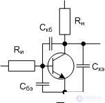
Figure 1. Capacities of pn junctions in the simplest amplifier on a bipolar transistor
In this figure, the base transition capacitance is designated Cb, and the collector junction capacitance is indicated Ckb. In order to evaluate only the frequency characteristics of the amplifier stage, the transistor is replaced by an equivalent circuit. The equivalent transistor circuit is shown in Figure 2.
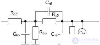
Figure 2. Equivalent transistor circuit
Based on the equivalent circuit shown in Figure 2, the frequency properties of the amplifier stage assembled on the transistor can be described by an RC chain, the resistance of which will consist of connecting the output impedance of the previous amplification stage (or output impedance of the signal source) in series and the input capacitance of the subsequent amplification stage.
If the voltage at the output of the transistor corresponded to zero voltage, then the input current of the transistor was determined by the sum of the currents through the capacitors Ccb and Cb. In this case, the input capacitance could be replaced by a parallel connection of these capacitors. In fact, the voltage at the output of the amplifying device is a factor times the input voltage and is opposite in sign. This voltage is applied to the plates of capacitance Ckb. As a result, the current through this capacitance will be a factor of more times, which is equivalent to increasing the capacitance by the appropriate number of times. This phenomenon is called the Miller effect. The value of the input capacitance of the transistor taking into account the Miller effect can be determined by the following formula:
As already mentioned above, the input capacitance determines the frequency response of the transistor amplification stage. Therefore, an increase in the input capacitance of the amplifier stage due to the Miller effect leads to a sharp deterioration in the frequency characteristics of the inverting amplifier. This makes it necessary to combat the Miller effect using various circuit solutions.
Usually, amplifiers with a voltage gain Ku equal to unity are used to combat the Miller effect. The gain of these cascades over current should naturally be significantly greater than one. As such cascades, it is possible to call the switching circuit with a common collector and with a common emitter working for a load resistance equal to RL = 1 / Soo. For field-effect transistors, these will be switching circuits with a common drain and a common source, respectively.
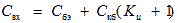
Suppressing the Miller effect using a common-collector circuit (emitter follower) is usually used in an op amp circuit. In these circuits, simultaneously with a decrease in the input capacitance, the input resistance of the emitter follower increases, which makes it possible to increase the gain of the previous stage to a value several thousand times. An example of a circuit with Miller effect suppression using an emitter follower is shown in Figure 3.
Figure 3. Schematic diagram with the suppression of the Miller effect using an emitter follower
In this scheme, the Miller effect is suppressed for the cascade assembled on the transistor VT2. As a result, the frequency response of the voltage amplifier assembled on the transistor VT1 will be determined by the high output impedance of this stage and the small input capacitance of the next stage assembled on the transistor VT2.
In high-frequency circuits of radio frequency amplifiers, the OE-OB suppression circuit has gained widespread acceptance, which has received a special name, the cascode circuit. A similar scheme is shown in Figure 4.
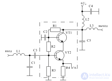
Figure 4. Cascode Miller effect suppression circuit
In this scheme, the same current flows through the OE and ON cascades, therefore the input resistance of the cascade with ON will be inversely proportional to the slope of the cascade with the common emitter. The voltage gain of the first stage is determined by the product of the slope and the load resistance, and therefore in this case will be equal to unity. The first cascade, assembled according to the scheme with OE, will amplify the input signal only by current. Gain voltage across the circuit as a whole will be determined by a cascade with the ON, collected on the transistor VT1. And since the first cascade does not possess voltage amplification, the Miller effect does not manifest itself in this scheme.
It should be noted that the Miller effect is manifested not only in transistor amplifiers, but also in any inverting amplifiers. In this case, an increase in the input capacitance can be both undesirable and a useful property. As an example, an integrator circuit, performed on an operational amplifier. An integrator on an operational amplifier using the Miller effect is shown in Figure 4.
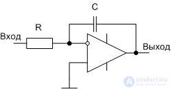
Figure 5. Schematic diagram of the integrator on the operational amplifier
In this integrator circuit, the value of capacitance C increases by a factor of a factor. For an op amp this can be up to 50,000 times! As a result, instead of an unstable electrolytic capacitor, a compact and cheap ceramic capacitor can be used in the integrator circuit to implement the integration function.

Comments
To leave a comment
Electrical Engineering, Circuit design
Terms: Electrical Engineering, Circuit design