Lecture
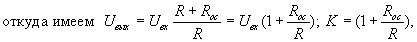
Basic ratio
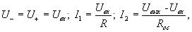
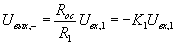
We assume that the OS has the properties of an ideal OS. The main type of environmental protection is parallel negative voltage feedback with the inclusion of additional resistance. The generalized scheme of OS with environmental protection is presented in Figure 4.
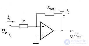
Pic.4
Given the virtual zeros of the OU, we have: 
From here
. 
Thus, the transmission coefficient of the circuit is
 .
.
It is determined only by external resistances; therefore, any given value can be realized, so this type of circuit is called an inverting scale amplifier.
Inverting adder with a given weighting factor
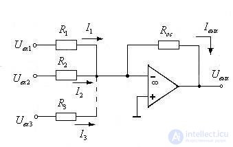
Pic.5
Since the OS operates in the linear mode, the superposition method can be used to determine the U out : you can get the U out as the sum U o , n. Considering the fact that the input current of the OU is zero, we have  , In this way,
Adder could be performed without the use of OU. However, in this case, the result would depend on the load resistance, and Uout would be much smaller than any of the U in .
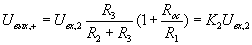
Non-inverting amplifier
(Generalized diagram 2)
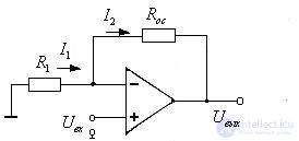
Fig. 6
 |
 |
 |
This circuit is called a non-inverting scale amplifier. Since the feedback voltage is fed to the inverting input here, and the signal is fed to the non-inverting input, the input resistance of the circuit is very high.
Non-inverting repeater
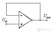
Fig. 7
Here 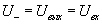 . This circuit has the advantages of an ideal voltage follower with very high input and very low output impedances.
Subtractor
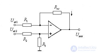
Fig. eight
 |
 |
Consequently, 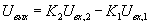 i.e. the circuit performs the subtraction operation.
Linear combination of input signals.
In some cases, it is necessary to add and subtract signals with different weights. By combining the circuits of the subtractor and the adder one can obtain the corresponding devices (see Fig. 9).
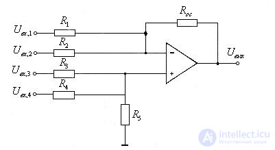
Fig. 9

which means a linear combination of signals with given coefficients.
Integrator
 but)
but) 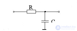 b)
b)
Fig. ten
Let us determine the frequency transfer characteristic of the circuit of fig. 10, a, applying the basic ratio for the harmonic input signal. For this scheme, the frequency transfer ratio
. 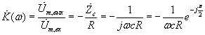
The type of transmission coefficient indicates that this circuit integrates the input signal. A similar conclusion can be obtained by writing the expression for the currents:
Figure 11 shows the frequency response of the integrator with the OS, and the frequency response of the passive integrating RC chain (Figure 10b), the transmission coefficient of which is described by the relation

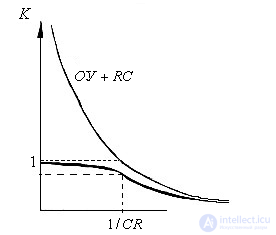
Fig. eleven
From fig. 11 that the integration region of the integrator with the OS is much wider than the integration region of the simplest RC chain, for which the integration region is w >> 1 / RC.
Differentiator
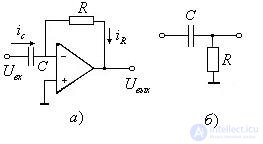
Fig. 12
For the circuit fig. 12, but you can write:

On the other hand, the frequency gain of the differentiator with an OS is equal to  that in the frequency domain characterizes the perfect differentiation.
For passive RC-chain fig. 12, b

Figure 13 shows the frequency response of differentiators with OU and without OU.
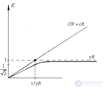
Fig. 13
In the CR chain, the differentiation region is bounded above by the frequency 
Logarithm and anti-log amplifiers
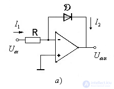
Fig. 14
VAC diode when U D > 0 is described by the equation
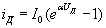
From equality  we have
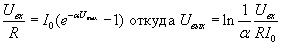
For U in <0 you should change the polarity of the diode. By setting the subsequent scale gain, you can change the base of the logarithm. For the scheme of Figure 14, we have
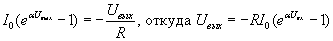
those. the circuit performs an antilog operation.
Multiplier
The use of diagrams fig. 14 a, b allows to perform such a seemingly non-linear transformation as multiplication. Figure 15 shows a block diagram of such a device.
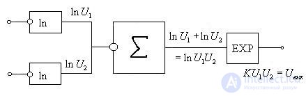
Fig. 15

Comments
To leave a comment
Electrical Engineering, Circuit design
Terms: Electrical Engineering, Circuit design