Lecture
The three-state logic element circuit is borrowed from the monograph [8] and slightly modified taking into account the capabilities of the EWB program. The basic element of the 134 series is taken as a basis and an element is added to it, which makes it possible to implement the third state mode or the so-called Z-state. It should be noted that the element under consideration is an important component of many digital ICs, from the simplest logic elements (for example, K155LA9) to complex registers and bus drivers, which provide the possibility of implementing the most common computer architectures and microprocessor control systems with a common bus.
The circuit diagram of a logic element with three states is presented in Fig. 9.15. It contains the basic logic element of the 134 series on transistors VT1 ... VT4, resistors R1 ... R4 and a diode VD2. In the basic element, the so-called multi-emitter transistor is used as VT1, however, due to the lack of such in the EWB library, it is represented by a conventional transistor. An input signal simulator on switch D is connected to the input In of the logic element, controlled by the D key from the keyboard, a resistor Rd simulating the output resistance of a logic zero source, and a voltage source V = + 5 V with an internal resistance of 1 kOhm simulating an input signal in the generation mode logical unit. The diode VD1 is connected to point A of the circuit in a simulator of the source for controlling the state of the output of a logic element on switch E controlled by the key E. All elements of the additional circuit are components from the Passive and Control libraries. In the initial state, the diode VD1 is closed by a voltage of positive polarity at its cathode and it does not affect the operation of the circuit. A resistor Rd is connected to the emitter of transistor VT1, on which a voltage drop is created
 (9.1)
(9.1)
where Uss = 5V is the supply voltage; Ube = 0.7 V - base-emitter voltage of an open transistor.
At
 (9.2)
(9.2)
the logic element perceives the input signal as a logic zero signal. In this case, the voltage at the collector of transistor VT1 and base VT2 is not enough to open the latter. As a result, the voltage drop across the resistor R3 is close to zero and the transistor VT4 will be closed, and the base of the transistor VT3 is connected to the power supply Ucc through the resistor R2 and VT3 will be open. In this case, the output voltage Uy, measured by a multimeter, is approximately equal to
 (9.3)
(9.3)
where Ukbnas <1 V is the saturation voltage of the transistor VT4; Uп
If we choose Ry >> R4, then Uy> 3 V, i.e. when a logical zero signal is applied to the input, the output will be a logical unit signal. Thus, the circuit in Fig. 9.15 is a logical element NOT (inverter).
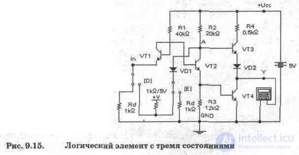
When the D key switches the same switch to a different position, the logic unit signal is applied to the emitter of transistor VT1, as a result of which the emitter junction is closed, and transistor VT1 is converted to inverse mode. In this case, under the action of the current flowing through the base-collector circuit VT1, the transistor VT2 opens and due to the voltage drop across the resistors R2, R3, the transistor VT3 closes, and VT4 opens, and a logic zero signal is established at the output Y.
When translating the same-name switch with the E key to the second position, the collector voltage of the transistor VT2 (point A) will be equal to
 (9.4)
(9.4)
When the inequality R2 >> Rd is satisfied, the voltage is Uп
In addition to demonstrating the considered modes of the circuit, it can also be used to study:
About noise immunity at the main input and the input of the third state resolution by varying the resistance Rd taking into account expressions (9.1), (9.2) and (9.4);
On the effect of load resistance on the amplitude of the output voltage of the valve when generating a signal of a logical unit by changing the input resistance of the multimeter taking into account expression (9.3);
About the influence of the load resistance connected between the output and the power supply bus Ucc on the output voltage of the valve when generating a logic zero signal;
On the effect of capacitive loading on the shape and amplitude of the output signal of the valve;
in this case, it is necessary to connect a capacitor of variable capacitance and an oscilloscope to the output, and to generate rectangular signals, hold the D key, while the pulse repetition rate will be equal to the symbol repetition rate for this keyboard;
About a similar element with three states in the faster series 155, for which the resistance of all resistors must be reduced by 10 times.
Note that the component library contains a non-inverting element with three states. It is shown in fig. 9.16, where it is indicated: In, Out, Enable - input, output and input of the enable signal. When a logical zero is applied to the permission input, the buffer output is transferred to the third state.
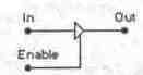
Fig. 9.16. Three-state buffer element
In conclusion, we mention the open collector logic element. Its scheme differs from fig. 9.15 in that it does not have a VT3 transistor, and the collector of a VT4 transistor is connected to one of the external terminals. To this terminal, a supply voltage is supplied through the load resistor, which can exceed the supply voltage of the entire IC.
Test questions and tasks
1. What are the remarkable properties of a logic element with three states, what tasks of digital technology did it solve?
2. Research the logic element in fig. 9.15 in accordance with the recommendations at the end of the section.

Comments
To leave a comment
Digital devices. Microprocessors and microcontrollers. computer operating principles
Terms: Digital devices. Microprocessors and microcontrollers. computer operating principles