Lecture
Cache [1] [2] [3] or cache [4] [5] [6] (English cache , from French cacher - “hide”; pronounced [kæʃ] - “cache”) - intermediate buffer with fast access containing information that is most likely to be requested. Access to data in the cache is faster than fetching source data from a slower memory or a remote source, but its volume is significantly limited compared to the source data storage.
For the first time the word “cache” in a computer context was used in 1967 during the preparation of an article for publication in the journal “IBM Systems Journal”. The article dealt with improvements in memory in the developed model 85 of the IBM System / 360 series. Magazine editor Lyle Johnson asked for a more descriptive term than “high-speed buffer,” but because of the lack of ideas, he suggested the word “cache”. The article was published in early 1968, the authors were awarded by IBM, their work became widespread and subsequently improved, and the word “cache” was soon used in computer literature as a generally accepted term. [7]
A cache is a memory with a higher access speed, designed to speed up access to data that is kept permanently in memory with a lower access speed (hereinafter referred to as “main memory”). Caching is used by the CPU, hard drives, browsers, web servers, DNS, and WINS.
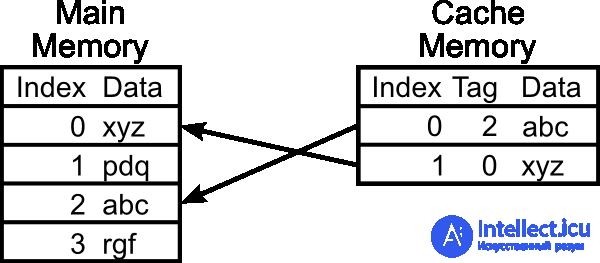
A cache consists of a set of entries. Each record is associated with a data item or a data block (a small part of the data), which is a copy of the data item in main memory. Each entry has an identifier that defines the correspondence between data items in the cache and their copies in main memory.
When a cache client (CPU, web browser, operating system) accesses data, the cache is first examined. If an entry in the cache is found with an identifier that matches the identifier of the requested data element, then the data elements in the cache are used. This is called a cache hit . If an entry containing the requested data item is not found in the cache, then it is read from the main memory in the cache, and becomes available for subsequent accesses. This is called a cache miss . The percentage of accesses to the cache when a result is found in it is called the hit level or cache hit ratio .
For example, a web browser checks the local disk cache for a local copy of a web page that matches the requested URL. In this example, the URL is the identifier, and the content of the web page is the data item.
If the cache is limited in size, then in case of a miss, it may be decided to discard some entry to free up space. Different preemption algorithms are used to select the record to be dropped.
When modifying data items in the cache, they are updated in the main memory. The time delay between modifying data in the cache and updating the main memory is controlled by a so-called write policy .
In an immediate write cache, each change causes a synchronous update of data in the main memory.
In the write - back (or write-back ) cache, an update occurs when a data item is preempted, periodically or at the request of a client. To keep track of modified data items, cache entries store a modification sign ( modified or “dirty” ). A deferred cache miss may require two accesses to main memory: the first to write replaceable data from the cache, the second to read the required data item.
In case the data in the main memory can be changed independently of the cache, the cache entry may become irrelevant . Inter-cache communication protocols that maintain data consistency are called cache coherence protocols .
Due to the increase in the frequency at which the processors operate, and the increase in the performance of the RAM subsystem, the data transfer interface has become a bottleneck in the computing system.
Cache memory can give a significant performance gain in the case when the RAM clock frequency is much less than the processor clock frequency. A number of processor models have their own cache to minimize the access time to RAM (RAM), which is slower than registers (these registers and I / O buffers can be considered a zero-level cache). The clock speed for the cache is usually slightly less than the CPU frequency.
In processors with virtual addressing support, a small high-speed address translation buffer (TLB) is often introduced. His speed is important, as he is polled at every memory call.
The problem of synchronization between different caches (both single and multiple processors) is solved by the coherence of the cache.
There are three ways to exchange information between different levels of cache memory, or, as they say, cache architectures: inclusive, exclusive and non-exclusive.
Exclusive cache memory assumes the uniqueness of information located in different cache levels (preferred by AMD).
In non-exclusive caches can behave as you like.
The CPU cache is divided into several levels. The maximum number of caches is four. In the universal processor at the present time, the number of levels can reach three. The N + 1 cache is usually larger and slower in access speed and data transfer than the N cache.
One of the fundamental characteristics of cache memory - the level of associativity - displays its logical segmentation, which is due to the fact that sequential enumeration of all cache lines in search of the necessary data would require dozens of cycles and would nullify the entire gain from using the memory integrated in the CPU. Therefore, RAM cells are tightly bound to cache lines (each line can contain data from a fixed set of addresses), which significantly reduces search time.
With the same cache size, the scheme with the most associativity will be the least fast, but the most effective (after four-thread implementation, the increase in the “specific efficiency” per stream increases little).
Many peripheral storage devices use internal cache to speed up work, in particular, hard drives use cache memory from 1 to 64 MB (models with support for NCQ / TCQ use it for storing and processing requests), CD / DVD / BD-reader devices The disks also cache the read information to speed up reuse.
The operating system also uses part of the RAM as a cache of disk operations (for example, for external devices that do not have their own cache memory, including hard disks, flash memory, and floppy disks). Often all the free (not allocated to processes) RAM is provided for caching hard drives.
The use of caching external drives due to the following factors:
When reading, the cache allows you to read the block once, then store one copy of the block in RAM for all processes and display the contents of the block “instantly” (compared to a disk request). There is a technique of "pre-request" - in the background, the operating system also reads several next blocks in the cache (after the required one).
When writing the cache, you can group short entries into larger ones that are more efficiently processed by the drives, or avoid recording intermediate modifications. In this case, all intermediate states of the block are visible to the processes from the RAM.
Caching external storage devices significantly increases system performance by optimizing I / O utilization. The advantage of the technology is a transparent (imperceptible for programs) automatic optimization of the use of memory-disks with the invariance of the logic of applications working with files.
The disadvantage of write caching is the time lag between a write request from a program and the actual writing of a block to a disk, as well as a change in the order in which records are made, which can lead to information loss or inconsistency of structures during a power failure or system hang. This problem is smoothed by forced periodic synchronization (writing modified cache lines) and file system journaling.
When reading data, the cache memory gives an unambiguous performance gain. When recording data, the gain can be obtained only at the cost of reduced reliability. Therefore, one or another cache write policy may be selected in various applications.
There are two basic write cache policies: write-through and write-back:
Initially, all buffer headers are placed in the free buffer list. If a process intends to read or modify a block, then it executes the following algorithm:
The process reads the data into the received buffer and frees it. In case of modification, the process marks the buffer as “dirty” before release. When released, the buffer is placed in the head of the free buffer list.
In this way:
If the list of free buffers is empty, then the buffer preemption algorithm is executed. The preemption algorithm significantly affects the performance of the cache. The following algorithms exist:
The application of a particular algorithm depends on the data caching strategy. LRU is most effective if data is guaranteed to be reused soon. MRU is most effective if the data is guaranteed not to be reused soon. In case the application explicitly specifies a caching strategy for a certain set of data, then the cache will function most efficiently.
RAM cache consists of the following elements:
The process of transferring information over the network can use caching of Internet pages — the process of storing frequently requested documents on (intermediate) proxy servers or a user's machine, in order to prevent their constant download from the source server and to reduce traffic. Thus, the information moves closer to the user. Caching is managed using HTTP headers.
Alternatively, caching of web pages can be performed using a CMS of a specific site to reduce server load with high attendance. Caching can be done both in memory and in the file cache [8] . The lack of caching is that changes made on one browser may not immediately be reflected in another browser, in which data is taken from the cache.
Many programs write somewhere intermediate or auxiliary results of the work, so as not to calculate them every time they are needed. This speeds up the work, but requires additional memory (operational or disk). An example of such caching is database indexing.
It makes sense to equip your multi-core processor with dedicated memory for use by all available cores. In this sense, fast L3 cache can provide quick access to the necessary data. Kernels should not need a slow computer RAM.
This is at least a theory. The recent AMD test Athlon II X4 which is practically the same Phenom II X4 only without a Level 3 memory cache, showed that L3 cache is not always so necessary. Kernels should not need slow RAM.
How does the cache work?
Before deep analysis of our tests, it is necessary to understand some basic concepts. The cache principle is pretty simple. Data is buffered as close as possible to the kernel in order to avoid memory swapping from slow sources at long distances.
Requests for data that can be answered within this cache are called hits. If the cache does not contain the data you are looking for and you must go through a request for subsequent memory structures, these are Missas. Modern computers have a margin of 3 cache levels before they start using slow system memory. The second and especially 3 levels of cache memory serve not only for buffering data. Their goal is also to prevent overloading the processor bus during data exchange between the cores.
Hit / miss cache
Эффективность кэш архитектуры измеряется понятием Хит рэйта- hit rate. Запрос данных который может быть прочитан с кэша называется hit. Miss-данные которые не могут быть взяты с кэша, эти данные берутся с системной медленной памяти. Другими словами Хиты делают работу быстрой а Мисы медленной.
Кэш Writes, Exclusivity, Coherency
Политика замены "занимается" распределением новой, входящей в кэш, информации. Информация записанная в кэш должна быть доступна и в системной памяти. Система может либо перезаписать новую информацию в кэш или отметить место перезаписанной информации как "грязным", тем самым давай системе понять что данное место кэша можно освободить.
Данные на разных уровнях кэша хранятся единственно, это означает отсутствие избыточности. Тоесть вы не найдете одни и те же данные на разных уровнях кэша. Кроме того, кэш может работать всеобъемлюще, кэш более низкого уровня может взаимодействовать с кэшем более высокого уровня. Phenom AMD работает с эксклюзивным L3 кэшем, в то время как Intel следует стратегии инклюзивного кэша. Слаженность протоколов заботиться о сохранении данных на нескольких уровнях, ядрах, и даже процессорах.
Объем кэша
Кэш большего размера хранит больше информации, но тут как правило фигурируют более высокие задержки. Так как кэш требует большое количество процессорных транзисторов, важно найти баланс между стоимостью транзисторов и их жизненным ресурсом, энергопотреблением и производительностью.
Associativity
Кэш-память N-канальной ассоциативности означает, что информация, размещённая по неком адресу оперативной памяти, может кэшироваться в N местах этой кэш-памяти. Высшая ассоциация обеспечивает лучшую гибкость кэширования, потому, что существующие кэш данные не нуждаются в перезаписи. Другими словами высшая N-канальная ассоциативность обеспечивают высокие Хит-рэйты, но при этом увеличивают задержки, потому что сравнение ассоциаций хитов занимает больше времени. Многоканальная ассоциация имеет смысл для кэша последних уровней потому, что тут сосредоточена основная емкость кэша, и это снимает потребность процессора работать с более медленной оперативной памятью.
Несколько примеров: Процессоры Core I5 и Core I7 работают с 32Кб 8-канальным ассоциативным кэшем 1-го уровня и 32Кб 4-канального ассоциативного кэша инструкций 1-го уровня. Ясно, что Intel хочет что б инструкции выполнялись быстрее одновременно увеличивая количество хитов кэша 1-го уровня. Кэш 2-го уровня тоже 8-ми канальный. Кэш 3-го уровня несколько умнее, тут внедрен 16-канальный кэш который увеличивает количество хитов.
Однако, AMD следует другой политики в своих Phenom II X4, тут расположен 2-х канальный ассоциативный кэш первого уровня, что обеспечивает меньшие задержки. Что бы компенсировать возможные промахи увеличен объем памяти в два раза-64кб кэша данных и инструкция. Кэш память 2-го уровня такая же как у Intel. Но L3 кэш работает с 48-канальной ассоциативностью.
Of all this, it is impossible to judge a lot without looking at the entire processor architecture. Naturally, only benchmarks (performance tests) can show real results, and the meaning of this entire tour is to show the complexity of multi-level caching.

Comments
To leave a comment
Digital devices. Microprocessors and microcontrollers. computer operating principles
Terms: Digital devices. Microprocessors and microcontrollers. computer operating principles