Lecture
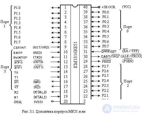
The microcontroller is made on the basis of high-level n-MOS technology and is available in an LSI package with 40 external leads. The pinout of the MK51 case and the names of the conclusions are shown in fig. 3.1 . For operation, the MK51 requires one +5 V power supply. Through four programmable I / O ports, the MK51 communicates with the medium in the three-state TTL circuit standard. The MK51 case has two pins for connecting a quartz resonator, four pins for signals that control the MK operation mode, and eight port 3 lines that can be programmed by the user to perform specialized (alternative) information exchange functions with the medium.
The basis of the MK51 structural diagram ( Fig. 3.2 ) is formed by an internal bidirectional 8-bit bus that interconnects all the main nodes and devices: resident memory, ALU, special function register block, control device, and input / output ports. Consider the basic elements of the structure and features of the organization of the computational process in MK51.
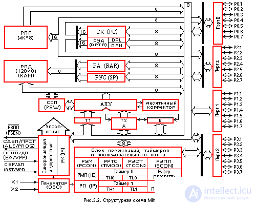
8-bit ALU can perform arithmetic operations of addition, subtraction, multiplication and division; logical operations AND, OR, exclusive OR, as well as operations of cyclic shift, reset, inversion, etc. In the ALU there are programmatically inaccessible registers T1 and T2, intended for the temporary storage of operands, the decimal correction scheme and the formation of signs.
The simplest addition operation is used in the ALU to increment the contents of the registers, advance the data-pointer register and automatically calculate the next RPF address. The simplest subtraction operation is used in the ALU to decrement registers and compare variables.
The simplest operations automatically form "tandems" for performing in the ALU such operations as, for example, incrementing 16-bit register pairs. The ALU implements a cascade mechanism for performing the simplest operations for implementing complex commands. So, for example, when executing one of the commands of conditional transfer of the board according to the comparison result in the ALU, the CS is incremented three times, the RPD is read twice, two variables are arithmetically compared, a 16-bit transition address is formed and the decision is made whether or not to proceed by program. All of the above operations are performed in the ALU in just 2 µs.
An important feature of the ALU is its ability to operate not only bytes, but also bits. Individual software-accessible bits can be set, reset, inverted, transmitted, tested, and used in logical operations. This ability of the ALU, to operate with bits, is so important that many descriptions of the MK51 state that it contains a "Boolean processor". To control objects, algorithms are often used that contain operations on input and output boolean variables (true / false), the implementation of which by means of ordinary microprocessors is associated with certain difficulties.
Thus, the ALU can operate with four types of information objects: boolean (1 bit), digital (4 bits), byte (8 bits) and address (16 bits). The ALU performs 51 different operations of sending or converting this data. Since 11 addressing modes are used (7 for data and 4 for addresses), by combining "operation / addressing mode" the basic number of commands 111 expands to 255 out of 256 possible with a single-byte operation code.
The program memory and data memory located on the MK5 chip are physically and logically separated, have different addressing mechanisms, work under control of different signals and perform different functions.
Program memory (ROM or EPROM) has a capacity of 4 KB and is designed to store commands, constants, initialization control words, conversion tables for input and output plug-ins, etc. RPT has a 16-bit address bus through which access is provided from the command counter or from the data pointer register. The latter performs the functions of a base register for indirect transitions in the program or is used in commands operating with tables.
The data memory (RAM) is intended for storing variables during the execution of an application program, addressed by one byte and has a capacity of 128 bytes. In addition, addresses of special function registers (RSF) are adjacent to the address space of the RPD, which are listed in Table 2.1 .
The program memory, as well as the data memory, can be expanded up to 64 Kbytes by connecting external LSIs.
Battery and SSP. The battery is the source of the operand and the place of fixation of the result when performing arithmetic, logical operations and a number of data transfer operations. In addition, only with the use of the battery can be performed the operation of shifts, checking for zero, the formation of the parity flag, etc.
Table 2.1. Special function register block
| Symbol | Name | Address |
| * ACC | Battery | 0E0H |
| * B | Battery Expander Register | 0F0H |
| * Psw | Program status word | 0D0H |
| SP | Stack Register | 81H |
| DPTR | Data Indicator Register (DPH) (Dpl) | 83H |
| 82H | ||
| * P0 | Port 0 | 80H |
| * P1 | Port 1 | 90H |
| * P2 | Port 2 | 0A0H |
| * P3 | Port 3 | 0B0H |
| * IP | Priority Register | 0B8H |
| * IE | Interrupt Mask Register | 0A8H |
| Tmod | Timer / Counter mode register | 89H |
| * TCON | Control register / timer status | 88H |
| TH0 | Timer 0 (high byte) | 8CH |
| Tl0 | Timer 0 (low byte) | 8AH |
| TH1 | Timer 1 (high byte) | 8DH |
| Tl1 | Timer 1 (low byte) | 8BH |
| * SCON | Transmitter Control Register | 98H |
| SBUF | Transceiver buffer | 99H |
| PCON | Power control register | 87H |
| Note. Registers whose names are marked with an asterisk ( * ) allow addressing of individual bits. | ||
During the execution of many commands in the ALU, a number of signs of the operation (flags) are formed, which are recorded in the MSP register. Table 2.2 provides a list of MTP flags, their symbolic names and the conditions for their formation.
Table 2.2. Format of the program status word (CSP)
Symbol | Position | Name and Purpose | |||
| C | PSW.7 | Carry flag Set and reset by hardware or program when performing arithmetic and logical operations | |||
| AC | PSW.6 | Auxiliary carry flag. It is set and reset only by hardware when performing addition and subtraction commands and signals a transfer or loan in bit 3 | |||
| F0 | PSW.5 | Flag 0. Can be set, cleared or checked by the program as a user-specified flag. | |||
RS1 RS0 | PSW.4 PSW.3 | The choice of bank registers. Set and reset by the program for selecting the working bank of registers (see note) | |||
| Ov | PSW.2 | Overflow flag. Set and reset by hardware when performing arithmetic operations | |||
_ | PSW.1 | Not used | |||
| P | PSW.0 | Parity flag The equipment is installed and reset in each command cycle and records an odd / even number of single bits in the battery, i.e. performs parity check | |||
| Note. | RS1 | RS0 | Bank | Address Bounds | |
| 0 | 0 | 0 | 00H-07H | ||
| 0 | one | one | 08H-0FH | ||
| one | 0 | 2 | 10H-17H | ||
| one | one | 3 | 18H-1FH | ||
The most "active" flag of the ERP is the hyphenation flag, which participates and is modified in the process of performing a set of operations, including addition, subtraction and translation. In addition, the carry flag (C) performs the functions of a "Boolean accumulator" in commands that manipulate bits. The overflow flag (OV) fixes arithmetic overflow in operations with signed integers and makes it possible to use arithmetic in additional codes. The ALU does not control the selection flags of the bank of registers (RS0, RS1), and their value is fully determined by the application program and is used to select one of four register banks.
The idea that in microprocessors, whose architecture relies on a battery, most of the teams work with it using the default (implicit) addressing has become widespread. In MK51, the situation is different. Although the processor in the MK51 is based on a battery, however, it can execute many commands without the participation of the battery. For example, data can be transferred from any cell of the RAP to any register, any register can be loaded with an immediate operand, etc. Many logical operations can be performed without battery power. In addition, variables can be incremented, decremented and verified (test) without using a battery. Flags and control bits can be checked and modified in the same way.
Register registers. The 8-bit stack pointer (RUS) can address any region of the RAP. Its contents are incremented before data is stored on the stack during the execution of the PUSH and CALL commands. The contents of the RUS are decremented after executing the POP and RET commands. This way of addressing stack elements is called pre-increment / post-dekrement. In the process of initializing the MK51, after the signal from the SSR, code 07H is automatically loaded into the ENG This means that if the application does not override the stack, then the first data element in the stack will be located in the RAP cell with the address 08H.
A two-byte data register-pointer (RUD) is usually used to fix a 16-bit address in operations with external memory access. With the MK51 commands, the data register-pointer can be used either as a 16-bit register or as two independent 8-bit registers (DPH and DPL).
Timer / Counter. The MK51 tools include register pairs with the symbolic names TNO, TLO and THI, TLI, on the basis of which two independent software-controlled 16-bit event timers / counters operate.
Serial port buffer. The register with the symbolic name SBUF consists of two independent registers - the buffer of the receiver and the buffer of the transmitter. Loading a byte into the SBUF immediately triggers the start of the transfer process via the serial port. When a byte is read from the SBUF, it means that its source is the serial port receiver.
Special function registers. Registers with symbolic names IP, IE, TMOD, TCON, SCON and PCON are used to fix and programmatically change the control and status bits of the interrupt circuit, timer / counter, serial port transceiver, and power control for the MK51. Their organization will be described below when considering the features of the MK51 operation in various modes.
A quartz resonator connected to the external terminals X1 and X2 of the MK51 case controls the operation of the internal oscillator, which in turn generates synchronization signals.
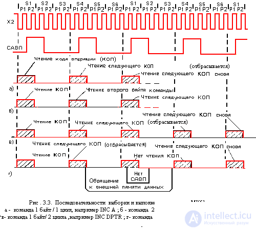
a - command 1 byte / 1 cycle, for example INC A; b - command - 2 bytes / 1 cycle, for example ADD A, #d; c - command 1 byte / 2 cycles, for example INC DPTR; g - command 1 byte / 2 cycles, for example MOVX.
Based on the synchronization signals, the MK51 control device forms a machine cycle of a fixed duration equal to 12 periods of the resonator or six states of the primary control automaton (S1_S6). Each state of the control automat contains two phases (P1, P2) of the resonator signals. In the P1 phase, as a rule, an operation is performed in the ALU, and in the P2 phase, an interregister transmission is performed. The entire machine cycle consists of 12 phases, starting with the S1P1 phase and ending with the S6P2 phase, as shown in fig. 3.3 . This timing diagram illustrates the operation of the MK51 control unit when sampling and executing commands of varying degrees of complexity. All shaded signals are internal and inaccessible to the user MK51 for control. External, observed signals are only the signals of the resonator and the gate address of the external memory. As can be seen from the timing diagram, the CELP signal is generated twice in one machine cycle (S1P2-S2P1 and S4P2-S5P1) and is used to control the process of accessing external memory.
Most of the MK51 commands are executed in one machine cycle. Some commands that operate on 2-byte words or are associated with accessing external memory are executed in two machine cycles. Only division and multiplication commands require four machine cycles. On the basis of these features of the operation of the control device MK51, the time of execution of the application programs is calculated.
The MK51 command system contains 111 basic commands, which are conveniently divided into five groups according to the functional feature: data transfer commands, arithmetic operations, logical operations, control transfers, and bit operations.
The MK51 command system is much more powerful and wider than the MK48 command system, since besides all the MK48 commands, it includes multiplication, division, subtraction, bit operations, stack operations and an extended set of control transfer commands. Most of the commands (94) are in the format of one or two bytes and are executed in one or two machine cycles. At a clock frequency of 2 MHz, the machine cycle duration is 1 μs. In fig. 3.19 shows 13 types of commands MK51. The first byte of the command of any type and format always contains an operation code (COP). The second and third bytes contain either the addresses of the operands, or the immediate operands.
Types of operands. The composition of the MK51 operands is wider than the MK48, and includes operands of four types: bits, 4-bit digits, bytes and 16-bit words.

Unlike the MK48, which has only three bit flags, the MK51 has 128 program-controlled user flags. It is also possible to address individual bits of the register of special functions and ports. For addressing a bit, a direct 8-bit address (bit) is used. Indirect bit addressing is not possible. Map addresses of individual bits are presented in Figure 3.20 and Figure 3.21 . Four-bit operands are used only for exchange operations (SWAP and XCHD commands). The eight-bit operand can be a program or data memory cell (resident or external), a constant (direct operand), special function registers (RSF), and input / output ports. Ports and RSF are addressed only in a direct way. Memory bytes can also be addressed indirectly via address registers (R0, R1, DPTR and PC). Double-byte operands are constants and direct addresses, which are represented by the second and third bytes of the command.
Ways of addressing data. MK51 uses the same methods of addressing data as MK48: direct, direct, indirect and implicit. It should be noted that in the indirect method of addressing the RPD, in contrast to MK48, all eight bits of the address registers R0 and R1 are used.
Compared to MK48, the command system MK51 allows more combinations of addressing operands in commands, which makes it more flexible and versatile.
Result flags. The program status word (PSW) includes four flags: C - carry, AC - auxiliary carry, O - overflow, and P - parity.
The parity flag (not in MK48) is directly dependent on the current value of the battery. If the number of single bits of the battery is odd, then the P flag is set, and if even - resetting attempts to change the P flag, assigning it a new value, will be unsuccessful if the contents of the battery remain unchanged.
The AC flag is set if a transfer / loan occurred between the tetrads of a byte during the operation of addition / subtraction.
The C flag is set if a carry or loan occurs in the high-order bit of the result. When performing multiplication and division operations, the C flag is cleared. The OV flag (absent in MK48) is set if the result of the addition / subtraction operation does not fit in seven bits and the upper (eighth) bit of the result cannot be interpreted as sign. When performing a division operation, the OV flag is cleared, and in the case of division by zero, it is set. When multiplying, the OV flag is set if the result is greater than 255.
In tab. 3.1 lists the commands for which the result flags are modified. The table does not have a parity flag, since its value is changed by all commands that change the contents of the battery. In addition to the commands listed in the table, the flags are modified by commands in which the destination of the result is defined by the PSW or its individual bits, as well as by the commands for operations on the bits.
Table 3.1. Commands that modify result flags
Teams | Flags | Teams | Flags | |
| ADD | C, OV, AC | CLR C | C = 0 | |
| ADDC | C, OV, AC | CPL C | C = m C | |
| SUBB | C, OV, AC | ANL C, b | C | |
| MUL | C = 0, OV | ANL C, / b | C | |
| Div | C = 0, OV | ORL C, b | C | |
| DA | C | ORL C, / b | C | |
| RRC | C | MOV C, b | C | |
| RLC | C | Cjne | C | |
| SETB C | C = 1 |
Symbolic addressing. При использовании ассемблера МК51 (ASM51) для получения объектных кодов программ допускается применение в программах символических имен регистров специальных функций (РСФ), портов и их отдельных бит ( рис. 3.21 ).
Для адресации отдельных бит РСФ и портов (такая возможность имеется не у всех РСФ) можно использовать символическое имя бита следующей структуры:
< имя РСФ или порта > . < номер бита >
Например, символическое имя пятого бита аккумулятора будет следующим: АСС.5. Символические имена РСФ, портов и их бит являются зарезервированными словами для ASM51, и их не надо определять с помощью директив ассемблера.
|
|
Большую часть команд данной группы ( табл. 3.2 ) составляют команды передачи и обмена байтов. Команды пересылки бит представлены в группе команд битовых операций. Все команды данной группы не модифицируют флаги результата, за исключением команд загрузки PSW и аккумулятора (флаг паритета).
Структура информационных связей. В зависимости от способа адресации и места расположения операнда можно выделить девять типов операндов, между которыми возможен информационный обмен. Граф возможных операций передачи данных показан на рис. 3.22 . Аккумулятор (А) представлен на этом графе отдельной вершиной, так как многие команды используют неявную (подразумеваемую) адресацию.
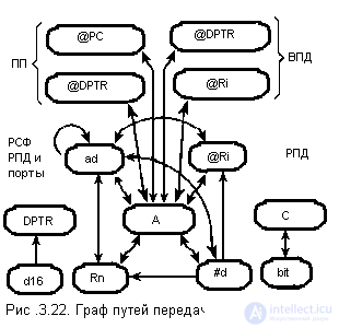
В отличие от МК48 передачи данных в МК51 могут выполняться без участия аккумулятора.
Аккумулятор. В отличие от МК48 обращение к аккумулятору может быть выполнено в МК51 с использованием неявной и прямой адресации. В зависимости от способа адресации аккумулятора применяется одно из символических имен: A или ACC (прямой адрес). При прямой адресации обращение к аккумулятору производится как к одному из РСФ, и его адрес указывается во втором байте команды.
Использование неявной адресации аккумулятора предпочтительнее, однако не всегда возможно, например при обращении к отдельным битам аккумулятора.
Обращение к внешней памяти данных. Режим косвенной адресации ВПД, имеющийся в МК48, реализован также и в МК51. При использовании команд MOVX @Ri обеспечивается доступ к 256 байтам внешней памяти данных.
Существует также режим обращения к расширенной ВПД, когда для доступа используется 16-битный адрес, хранящийся в ретистре-указателе данных (DPTR). Команды MOVX @DPTR обеспечивают доступ к 65 536 байтам ВПД.
Table 3.2. Группа команд передачи данных
Название команды | Мнемокод | КОП | T | B | C | Operation | |||||||||
| Пересылка в аккумулятор из регистра (n = 0 - 7) | MOV A, Rn | 11101rrr | one | one | one | (A) = (Rn) | |||||||||
| Пересылка в аккумулятор прямоадресуемого байта | MOV A, ad | 11100101 | 3 | 2 | one | (A) = (ad) | |||||||||
| Пересылка в аккумулятор байта из РДП (i = 0, 1) | MOV A, @Ri | 1110011i | one | one | one | (A) = ((Ri)) | |||||||||
| Загрузка в аккумулятор константы | MOV A, #d | 01110100 | 2 | 2 | one | (A) = #d | |||||||||
| Пересылка в регистр из аккумулятора | MOV Rn, A | 11111rrr | one | one | one | (Rn) = (A) | |||||||||
| Пересылка в регистр прямоадресуемого байта | MOV Rn, ad | 10101rrr | 3 | 2 | 2 | (Rn) = (ad) | |||||||||
| Загрузка в регистр константы | MOV Rn, #d | 01111rrr | 2 | 2 | one | (Rn) = #d | |||||||||
| Пересылка по прямому адресу аккумулятора | MOV ad, A | 11110101 | 3 | 2 | one | (ad) = (A) | |||||||||
| Пересылка по прямому адресу регистра | MOV ad, Rn | 10001rrr | 3 | 2 | 2 | (ad) = (Rn) | |||||||||
| Пересылка прямоадресуемого байта по прямому адресу | MOV add, ads | 10000101 | 9 | 3 | 2 | (add) = (ads) | |||||||||
| Пересылка байта из РДП по прямому адресу | MOV ad, @Ri | 1000011i | 3 | 2 | 2 | (ad) = ((Ri)) | |||||||||
| Пересылка по прямому адресу константы | MOV ad, #d | 01110101 | 7 | 3 | 2 | (ad) = #d | |||||||||
| Пересылка в РДП из аккумулятора | MOV @Ri, A | 1111011i | one | one | one | ((Ri)) = (A) | |||||||||
| Пересылка в РДП прямоадресуемого байта | MOV @Ri, ad | 0110011i | 3 | 2 | 2 | ((Ri)) = (ad) | |||||||||
| Пересылка в РДП константы | MOV @Ri, #d | 0111011i | 2 | 2 | one | ((Ri)) = #d | |||||||||
| Загрузка указателя данных | MOV DPTR, #d16 | 10010000 | 13 | 3 | 2 | (DPTR) = #d16 | |||||||||
| Пересылка в аккумулятор байта из ПП | MOVC A, @A + DPTR | 10010011 | one | one | 2 | (A) = ((A) + (DPTR)) | |||||||||
| Пересылка в аккумулятор байта из ПП | MOVC A, @A + PC | 10000011 | one | one | 2 | (PC) = (PC) + 1 (A) = ((A) + (PC)) | |||||||||
| Пересылка в аккумулятор байта из ВПД | MOVX A, @Ri | 1110001i | one | one | 2 | (A) = ((Ri)) | |||||||||
| Transfer to byte accumulator from extended vpd | MOVX A, @DPTR | 11100000 | one | one | 2 | (A) = ((DPTR)) | |||||||||
| Transfer to vpd from battery | MOVX @Ri, A | 1111001i | one | one | 2 | ((Ri)) = (A) | |||||||||
| Forward to Extended VAP from Battery | MOVX @DPTR, A | 11110000 | one | one | 2 | ((DPTR)) = (A) | |||||||||
| Load onto stack | Push ad | 11000000 | 3 | 2 | 2 | (SP) = (SP) + 1 ((SP)) = (ad) | |||||||||
| Fetch stack | Pop ad | 11010000 | 3 | 2 | 2 | (ad) = (sp) (SP) = (SP) - 1 | |||||||||
| Battery swap with register | XCH A, Rn | 11001rrr | one | one | one | (A) <-> (Rn) | |||||||||
| Battery swapping with direct byte | XCH A, ad | 11000101 | 3 | 2 | one | (A) <-> (ad) | |||||||||
| Exchange battery with byte from RDP | XCH A, @Ri | 1100011i | one | one | one | (A) <-> ((Ri)) | |||||||||
| Exchange of the low tetrad of the battery with the low tetra of the byte RDP | XCHD A, @Ri | 1101011i | one | one | one | (A 0-3 ) <-> ((Ri) 0-3 ) | |||||||||
Данную группу образуют 24 команды (табл. 3.3), выполняющие операции сложения, десятичной коррекции, инкремента/декремента байтов. Дополнительно по сравнению с МК48 введены команды вычитания, умножения и деления байтов.
Таблица 3.3. Группа команд арифметических операций
Название команды | Мнемокод | КОП | T | B | C | Operation |
| Сложение аккумулятора с регистром (n = 0 - 7) | ADD A, Rn | 00101rrr | one | one | one | (A) = (A) + (Rn) |
| Сложение аккумулятора с прямоадресуемым байтом | ADD A, ad | 00100101 | 3 | 2 | one | (A) = (A) + (ad) |
| Сложение аккумулятора с байтом из РПД (i = 0, 1) | ADD A, @Ri | 0010011i | one | one | one | (A) = (A) + ((Ri)) |
| Сложение аккумулятора с константой | ADD A, #d | 00100100 | 2 | 2 | one | (A) = (A) + #d |
| Сложение аккумулятора с регистром и переносом | ADDC A, Rn | 00111rrr | one | one | one | (A) = (A) + (Rn) + (C) |
| Сложение аккумулятора с прямоадресуемым байтом и переносом | ADDC A, ad | 00110101 | 3 | 2 | one | (A) = (A) + (ad) + (C) |
| Add a battery with a byte from the RPD and transfer | ADDC A, @Ri | 0011011i | one | one | one | (A) = (A) + ((Ri)) + (C) |
| Addition of battery with constant and carry | ADDC A, #d | 00110100 | 2 | 2 | one | (A) = (A) + #d + (C) |
| Battery decimal correction | DA A | 11010100 | one | one | one | If a (A 0-3 )> 9 \ / ((AC) = 1), then (A 0-3 ) = (A 0-3 ) + 6, then if (A 4-7 )> 9 \ / ((C) = 1), then (A 4-7 ) = (A 4-7 ) + 6 |
| Subtract battery from register and loan | SUBB A, Rn | 10011rrr | one | one | one | (A) = (A) - (C) - (Rn) |
| Subtracting from the battery direct address and byte | SUBB A, ad | 10010101 | 3 | 2 | one | (A) = (A) - (C) - ((ad)) |
| Deduction from the battery byte RPD and loan | SUBB A, @Ri | 1001011i | one | one | one | (A) = (A) - (C) - ((Ri)) |
| Вычитание из аккумулятора константы и заема | SUBB A, #d | 10010100 | 2 | 2 | one | (A) = (A) - (C) - #d |
| Инкремент аккумулятора | INC A | 00000100 | one | one | one | (A) = (A) + 1 |
| Инкремент регистра | INC Rn | 00001rrr | one | one | one | (Rn) = (Rn) + 1 |
| Инкремент прямоадресуемого байта | INC ad | 00000101 | 3 | 2 | one | (ad) = (ad) + 1 |
| Инкремент байта в РПД | INC @Ri | 0000011i | one | one | one | ((Ri)) = ((Ri)) +1 |
| Инкремент указателя данных | INC DPTR | 10100011 | one | one | 2 | (DPTR) = (DPTR) + 1 |
| Декремент аккумулятора | DEC A | 00010100 | one | one | one | (A) = (A) - 1 |
| Декремент регистра | DEC Rn | 00011rrr | one | one | one | (Rn) = (Rn) - 1 |
| Декремент прямоадресуемого байта | DEC ad | 00010101 | 3 | 2 | one | (ad) = (ad) - 1 |
| Декремент байта в РПД | DEC @Ri | 0001011i | one | one | one | ((Ri)) = ((Ri)) -1 |
| Умножение аккумуллятора на регистр B | MUL AB | 10100100 | one | one | four | (B)(A) = (A)*(B) |
| Деление аккумулятора на регистр B | DIV AB | 10000100 | one | one | four | (A).(B) = (A)/(B) |
Данную группу образуют 25 команд ( табл. 3.4 ), реализующих те же логические операции над байтами, что и в МК48. Однако в МК51 значительно расширено число типов операндов, участвующих в операциях.
Таблица 3.4. Группа команд логических операций
Название команды | Мнемокод | КОП | T | B | C | Operation |
| Логическое И аккумулятора и регистра | ANL A, Rn | 01011rrr | one | one | one | (A) = (A) /\ (Rn) |
| Логическое И аккумулятора и прямоадресуемого байта | ANL A, ad | 01010101 | 3 | 2 | one | (A) = (A) /\ (ad) |
| Логическое И аккумулятора и байта из РПД | ANL A, @Ri | 0101011i | one | one | one | (A) = (A) /\ ((Ri)) |
| Логическое И аккумулятора и константы | ANL A, #d | 01010100 | 2 | 2 | one | (A) = (A) /\ #d |
| Логическое И прямоадресуемого байта и аккумулятора | ANL ad, A | 01010010 | 3 | 2 | one | (ad) = (ad) /\ (A) |
| Логическое И прямоадресуемого байта и константы | ANL ad, #d | 01010011 | 7 | 3 | 2 | (ad) = (ad) /\ #d |
| Логическое ИЛИ аккумулятора и регистра | ORL A, Rn | 01001rrr | one | one | one | (A) = (A) \/ (Rn) |
| Логическое ИЛИ аккумулятора и прямоадресуемого байта | ORL A, ad | 01000101 | 3 | 2 | one | (A) = (A) \/ (ad) |
| Логическое ИЛИ аккумулятора и байта из РПД | ORL A, @Ri | 0100011i | one | one | one | (A) = (A) \/ ((Ri)) |
| Логическое ИЛИ аккумулятора и константы | ORL A, #d | 01000100 | 2 | 2 | one | (A) = (A) \/ #d |
| Логическое ИЛИ прямоадресуемого байта и аккумулятора | ORL ad, A | 01000010 | 3 | 2 | one | (ad) = (ad) \/ (A) |
| Логическое ИЛИ прямоадресуемого байта и константы | ORL ad, #d | 01000011 | 7 | 3 | 2 | (ad) = (ad) \/ #d |
| Исключающее ИЛИ аккумулятора и регистра | XRL A, Rn | 01101rrr | one | one | one | (A) = (A) \/ (Rn) |
| Исключающее ИЛИ аккумулятора и прямоадресуемого байта | XRL A, ad | 01100101 | 3 | 2 | one | (A) = (A) \/ (ad) |
| Исключающее ИЛИ аккумулятора и байта из РПД | XRL A, @Ri | 0110011i | one | one | one | (A) = (A) \/ ((Ri)) |
| Исключающее ИЛИ аккумулятора и константы | XRL A, #d | 01100100 | 2 | 2 | one | (A) = (A) \/ #d |
| Исключающее ИЛИ прямоадресуемого байта и аккумулятора | XRL ad, A | 01100010 | 3 | 2 | one | (ad) = (ad) \/ (A) |
| Исключающее ИЛИ прямоадресуемого байта и константы | XRL ad, #d | 01100011 | 7 | 3 | 2 | (ad) = (ad) \/ #d |
| Сброс аккумулятора | CLR A | 11100100 | one | one | one | (A) = 0 |
| Инверсия аккумулятора | CPL A | 11110100 | one | one | one | (A) = ( м A) |
| Сдвиг аккумулятора влево циклически | RL A | 00100011 | one | one | one | (A n+1 ) = (A n ), n = 0 ? 6, (A 0 ) = (A 7 ) |
| Сдвиг аккумулятора влево через перенос | RLC A | 00110011 | one | one | one | (A n+1 ) = (A n ), n = 0 ? 6, (A 0 ) = (C), (C) = (A 7 ) |
| Сдвиг аккумулятора вправо циклически | RR A | 00000011 | one | one | one | (A n ) = (A n+1 ), n = 0 ? 6, (A 7 ) = (A 0 ) |
| Сдвиг аккумулятора вправо через перенос | RRC A | 00010011 | one | one | one | (A n ) = (A n+1 ), n = 0 ? 6, (A 7 ) = (C), (C) = (A 0 ) |
| Обмен местами тетрад в аккумуляторе | SWAP A | 11000100 | one | one | one | (A 0-3 ) <-> (A 4-7 ) |
Отличительной особенностью данной группы команд ( табл. 3.5 ) является то, что они оперируют с однобитными операндами. В качестве таких операндов могут выступать отдельные биты некоторых регистров специальных функций (РСФ) и портов, а также 128 программных флагов пользователя.
Таблица 3.5. Группа команд операции с битами
Название команды | Мнемокод | КОП | T | B | C | Operation |
| Сброс переноса | CLR C | 11000011 | one | one | one | (C) = 0 |
| Сброс бита | CLR bit | 11000010 | four | 2 | one | (b) = 0 |
| Установка переноса | SETB C | 11010011 | one | one | one | (C) = 1 |
| Установка бита | SETB bit | 11010010 | four | 2 | one | (b) = 1 |
| Инверсия переноса | CPL C | 10110011 | one | one | one | (C) = ( м C) |
| Инверсия бита | CPL bit | 10110010 | four | 2 | one | (b) = ( m b) |
| Logical and bit and carry | ANL C, bit | 10000010 | four | 2 | 2 | (C) = (C) / \ (b) |
| Logical and bit inversion and carry | ANL C, / bit | 10110000 | four | 2 | 2 | (C) = (C) / \ ( m b) |
| Logical or bit and carry | Or C, bit | 01110010 | four | 2 | 2 | (C) = (C) \ / (b) |
| Logical OR bit inversion and carry | ORL C, / bit | 10100000 | four | 2 | 2 | (C) = (C) \ / ( m b) |
| Sending a bit to carry | MOV C, bit | 10100010 | four | 2 | one | (C) = (b) |
| Bit forwarding | MOV bit, C | 10010010 | four | 2 | 2 | (b) = (C) |
There are reset commands (CLR), settings (SETB) and inversion (CPL) bits, as well as conjunction and disjunction of the bit and carry flag. For addressing a bit, a direct eight-bit address (bit) is used. Indirect bit addressing is not possible.
This group of commands ( Table 3.6 ) includes commands providing conditional and unconditional branching, calling subroutines and returning from them, as well as the empty NOP operation command. Most commands use direct addressing, i.e. the entire transition address (or part thereof) is contained in the control transfer command itself. There are three types of branching commands according to the bit width of the indicated transition address.
Table 3.6. Control transfer command group
Team name | Mnemonic | KOP | T | B | C | Operation |
| Long transition in full memory in programs | LJMP ad16 | 00000010 | 12 | 3 | 2 | (PC) = ad16 |
| Absolute transition inside a page in 2 KB | AJMP ad11 | a 10 a 9 a 8 00001 | 6 | 2 | 2 | (PC) = (PC) + 2 (PC 0-10 ) = ad11 |
| Short relative transition within the page to 256 bytes | SJMP rel | 10,000,000 | five | 2 | 2 | (PC) = (PC) + 2 (PC) = (PC) + rel |
| Indirect relative transition | JMP @ A + DPTR | 01110011 | one | one | 2 | (PC) = (A) + (DPTR) |
| Jump if battery is zero | Jz rel | 01100000 | five | 2 | 2 | (PC) = (PC) + 2, if (A) = 0, then (PC) = (PC) + rel |
| Transition if the battery is non-zero | JNZ rel | 01110000 | five | 2 | 2 | (PC) = (PC) + 2, if (A)? 0, then (PC) = (PC) + rel |
| Transition, if the transfer is equal to one | JC rel | 01000000 | five | 2 | 2 | (PC) = (PC) + 2, if (C) = 1, then (PC) = (PC) + rel |
| Transition if the transfer is zero | JNC rel | 01010000 | five | 2 | 2 | (PC) = (PC) + 2, if (C) = 0, then (PC) = (PC) + rel |
| Jump if bit is one | JB bit, rel | 00100000 | eleven | 3 | 2 | (PC) = (PC) + 3, if (b) = 1, then (PC) = (PC) + rel |
| Transition if the bit is zero | JNB bit, rel | 00110000 | eleven | 3 | 2 | (PC) = (PC) + 3, if (b) = 0, then (PC) = (PC) + rel |
| Transition, if the bit is set, then reset the bit | JBC bit, rel | 00010000 | eleven | 3 | 2 | (PC) = (PC) + 3, if (b) = 1, then (b) = 0 and (PC) = (PC) + rel |
| Register decrement and transition if not null | DJNZ Rn, rel | 11011rrr | five | 2 | 2 | (PC) = (PC) + 2, (Rn) = (Rn) -1, if (Rn)? 0, then (PC) = (PC) + rel |
| Decrement of a direct-addressed byte and transition, if not null | DJNZ ad, rel | 11010101 | eight | 3 | 2 | (PC) = (PC) + 2, (ad) = (ad) -1, if (ad)? 0, then (PC) = (PC) + rel |
| Comparison of a battery with a direct-addressed byte and transition, if not equal | CJNE A, ad, rel | 10110101 | eight | 3 | 2 | (PC) = (PC) + 3, if (A)? (ad) then (PC) = (PC) + rel, if (A) <(ad), then (C) = 1, otherwise (C) = 0 |
| Compare battery with constant and transition if not equal | CJNE A, #d, rel | 10110100 | ten | 3 | 2 | (PC) = (PC) + 3, if (A)? #d, then (PC) = (PC) + rel, if (A) <#d, then (C) = 1, otherwise (C) = 0 |
| Register comparison with constant and transition, if not equal | CJNE Rn, #d, rel | 10111rrr | ten | 3 | 2 | (PC) = (PC) + 3, if (Rn)? #d, then (PC) = (PC) + rel, if (Rn) <#d, then (C) = 1, otherwise (C) = 0 |
| Comparison of bytes in the RPD with a constant and the transition, if not equal to | CJNE @Ri, #d, rel | 1011011i | ten | 3 | 2 | (PC) = (PC) + 3, if ((Ri))? #d, then (PC) = (PC) + rel if ((Ri)) <#d, then (C) = 1, otherwise (C) = 0 |
| Long subroutine call | LCALL ad16 | 00010010 | 12 | 3 | 2 | (PC) = (PC) + 3, (SP) = (SP) + 1, ((SP)) = (PC 0-7 ), (SP) = (SP) + 1, ((SP)) = (PC 8-15 ), (PC) = ad16 |
| Absolute subroutine call within a 2 KB page | ACALL ad11 | a 10 a 9 a 8 10001 | 6 | 2 | 2 | (PC) = (PC) + 2, (SP) = (SP) + 1, ((SP)) = (PC 0-7 ), (SP) = (SP) + 1, ((SP)) = (PC 8-15 ), (PC 0-10 ) = ad11 |
| Return from subroutine | RET | 00100010 | one | one | 2 | (PC 8-15 ) = ((SP)), (SP) = (SP) - 1, (PC 0-7 ) = ((SP)), (SP) = (SP) - 1 |
| Return from interrupt routine | RETI | 00110010 | one | one | 2 | (PC 8-15 ) = ((SP)), (SP) = (SP) - 1, (PC 0-7 ) = ((SP)), (SP) = (SP) - 1 |
| Single team | NOP | 00000000 | one | one | one | (PC) = (PC) + 1 |
| Note. The assembler allows the use of the generic name of the JMP and CALL commands, which are replaced in the process of translation by optimal call instructions (ACALL, LCALL) or transition (AJMP, SJMP, LJMP). | ||||||
Long transition . Navigate through the entire address space PP. The command contains the full 16-bit transition address (ad 16). Three byte long jump commands contain the letter L (Long) in the mnemonic. In total there are two such commands: LJMP - long transition and LCALL - long subroutine call. In practice, it is rarely necessary to navigate within the entire address space, and shorter transition commands are often used, taking up less space in memory.
Absolute transition. Transition within one page of program memory in the size of 2048 bytes. Such commands contain only 11 least significant bits of the transition address (ad 11). Absolute branch commands are 2 bytes long. The initial letter of the mnemonic is A (Absolute). When the command is executed in the calculated address of the following command ((PC) = (PC) + 2), the 11 lower bits are replaced by ad11 from the body of the absolute branch instruction.
Relative transition A short relative transition allows you to transfer control within -128 - +127 bytes relative to the address of the next command (the command following the order of the relative transition command). There is one unconditional short transition command SJMP (Short). All conditional jump commands use this addressing method. The relative address of the transition (rel) is contained in the second byte of the command.
Indirect transition. The JMP @A + DPTR command allows you to transfer control to an indirect address. This command is convenient in that it provides the possibility of organizing a transition to an address calculated by the program itself and unknown when writing the source code of the program.
Conditional transitions A developed system of conditional transitions allows branching according to the following conditions: a battery contains zero (JZ); battery content is not zero (JNZ); the transfer is equal to one (JC); carryover is zero (JNC); addressable bit is one (JB); the addressed bit is zero (JNB).
For organizing program cycles, it is convenient to use the DJNZ command, which works similarly to the corresponding MK48 command. However, as a loop counter in the MK51, not only the register can be used, but also direct-addressed bytes (for example, the RPD cell).
The CJNE command is effectively used in waiting for an event. For example, the command
WAIT: CJNE A, P0, WAIT
will be executed until the information on the lines of port 0 coincides with the contents of the battery.
All commands in this group, with the exception of CJNE and JBC, do not affect flags. The CJNE command sets the C flag if the first operand is less than the second. The JBC command clears the C flag in case of a transition.
Subprograms To access subroutines, you must use subroutine call commands (LCALL, ACALL). These commands, unlike the transition commands (LJMP, AJMP), save on the stack the return address to the main program. To return from a subroutine, you must issue the RET command. The RETI command differs from the RET command in that it enables interrupts of the served level.
All four ports MK51 are intended for input or output of information byte-by-byte. Circuitry I / O ports MK51 for one bit is shown in Fig. 3.4 (ports 1 and 2 have approximately the same structure as port 3). Each port contains a manageable latch, input buffer and output driver.
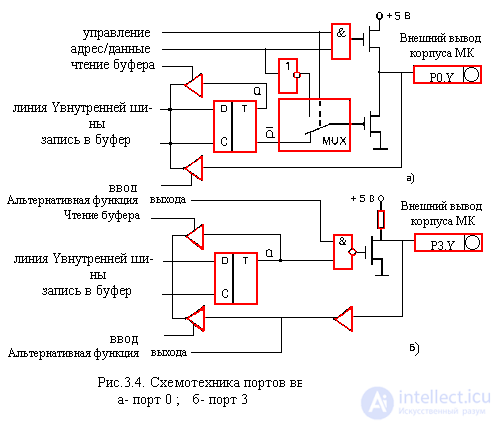
Output drivers of ports 0 and 2, as well as the input buffer of port 0, are used when accessing external memory (VP). In this case, through port 1 in time multiplexing mode, the low byte of the address of the VI is first output, and then the data byte is issued or received. Through port 2, the high byte of the address is output in cases when 1 address width is 16 bits.
All pins of port 3 can be used to implement alternative functions listed in table 8.1. Alternative functions can be enabled by writing 1 to the corresponding bits of the latch register (P3.0-P3.7) of port 3.
Table 8.1. Alternate Port 3 Features
Symbol | Position | Name and Purpose |
| m RD | P3.7 | Reading. The active low-level signal is formed by hardware when accessing the PDD |
| m wr | P3.6 | Record. The active low-level signal is formed by hardware when accessing the PDD |
| T1 | P3.5 | Timer / Counter 1 Input or Test Input |
| T0 | P3.4 | Timer / counter input 0 or test input |
| m int1 | P3.3 | Interrupt request input 1. A low level or cut signal is sensed. |
| m int0 | P3.2 | Interrupt request input 0. Low level signal or slice is perceived |
| Txd | P3.1 | Serial port transmitter output in UART mode. Shift register sync output |
| Rxd | P3.0 | Serial port receiver input in UART mode. Data input / output in shift register mode |
Port 0 is bidirectional, and ports 1, 2 and 3 are quasi-two-directional. Each port line can be used independently for input or output. In order for a port line to be used for input, a port latch must be written to the D-flip-flop of the port latch 1, which closes the MOSFET of the output circuit.
The signal of the RRF in the register-latch of all ports is automatically recorded units, thereby setting them to the input mode.
All ports can be used to organize the input / output of information on bidirectional transmission lines. However, ports 0 and 2 cannot be used for this purpose if the MK-system has an external memory, communication with which is organized via a common shared address / data bus operating in the time multiplexing mode.
Entry to the port. When executing a command that changes the contents of the port latch register, the new value is fixed in the register at the time of S6P2 of the last command cycle. However, the content of the latch register is polled by the output circuit during the P1 phase and, therefore, the new latch register content appears on the output pins of the port only at the time S1P1 of the next machine cycle.
Load capacity of ports. Output lines of ports 1, 2 and 3 can operate on a single TTL circuit. Port lines 0 can be loaded on two inputs of TTL circuits each. Port 0 lines can also work on n-MOS circuits, however, they must be connected to the power supply through external load resistors, except for the case when the port 0 bus is used as an external memory address / data bus.
Input signals for MK51 can be formed by TTL-circuits or n-MOS-circuits. Acceptable use as a source of signals for MK51 circuits with an open collector or open drain. However, at the same time, the time of change of the input signal at the transition from 0 to 1 will be much longer.
Features of the ports. Access to I / O ports is possible using commands operating with a byte, a separate bit and an arbitrary combination of bits. In this case, when the port is both an operand and a destination of the result, the control device automatically implements a special mode called read-modify-write. This mode of circulation involves input of signals not from external pins of the port, but from its register-latch, which allows to exclude incorrect reading of previously output information.
A similar mechanism for accessing ports is implemented in the following commands:
ANL - logical AND, for example ANL P1, A;
ORL - logical OR, for example, ORL P2, A;
XRL - exclusive OR, for example, XRL P3, A;
JBC - transition, if the address in the address bit is one, and the subsequent reset of the bit, for example JBC P1.1, LABEL;
CPL - bit inversion, for example, CPL P3.3;
INC — port increment, for example INC P2;
DEC — port decrement, for example, DEC P2;
DJNZ is the decrement of the port and the transition if its contents are not zero, for example DJNZ P3, LABEL;
MOV PX.Y, C - transfer of the carry bit to the Y bit of port X;
SET PX.Y - setting the Y bit of port X;
CLR PX.Y - reset the Y bit of port X.
It is not at all obvious that the last three commands in the list are "read-modify-write" commands. However, this is exactly the case. These commands first read a byte from the port, and then write a new byte into the register latch.
The reason why read-modify-write commands provide separate access to the port-latch and external pins of the port is the need to eliminate the possibility of incorrect reading of signal levels at external pins. Suppose, for example, that the Y line of port X is connected to the base of a powerful transistor and the output signal on it is intended to control it. When 1 is written to this bit, the transistor turns on. If to check the status of the actuator (in our case, the power transistor), the application program needs to read the output signal state in the same port bit, then reading the signal from the external output of the port, and not from the D-flip-flop of the port latch register will lead to the wrong result: a single signal at the base of the transistor has a relatively low level and will be interpreted in the MC as a signal 0. Commands "read-modify-write" realize reading from the register-latch, and not from the external output of the port, which ensures obtaining a correct value of 1.
In fig. 3.5 shows time diagrams illustrating the process of performing information input / output operations through the MK51 ports.

In microcontroller systems built on the basis of the MK51, it is possible to use two types of external memory: program permanent memory (WFP) and data random access memory (VPD). Access to the runway is carried out using the control signal of the MFAR, which performs the function of a strobe signal reading. Access to the VFD is provided by control signals m CHT and m ZP, which are formed in lines P3.7 and P3.6 when the port performs 3 alternative functions ( see Table 8.1 ).
When accessing the runway, a 16-bit address is always used. Access to the VFD is possible using a 16-bit address (MOVX A, @DPTR) or an 8-bit address (MOVX A, @Ri).
In any case of using a 16-bit address, the high byte of the address is fixed (and remains unchanged during one write or read cycle) in the port-latch register 2.
If the next cycle of external memory (MOVX A, @DPTR) does not immediately follow the previous cycle of external memory, the unchanged contents of the latch register of port 2 is restored in the next cycle. If an 8-bit address is used (MOVX A, @Ri), then the contents of the port-latch register of port 2 remain unchanged on its external pins during the entire cycle of external memory.
Through port 0 in time multiplexing mode, the low byte of the address is output and the data byte is transmitted. The signal SAWP must be used to write the address byte to the external register. Then, in the write cycle, the output data byte appears on the external pins of port 0 just before the appearance of the signal m ZP. In the read cycle, the input data byte is received at port 0 on the front of the strobe signal m THU.
With any access to external memory, the MK51 control unit loads the 0FFH code into the port 0 latch register, thereby erasing the information that could be stored in it.
Access to the runway is possible when two conditions are met: either an active signal is sent to the input to disable the resident program memory ( m EFS), or the command counter exceeds 0FFFH. The presence of the signal of the PPM is necessary to provide access to the lower 4K addresses of the address space of the runway when using the MK31 (microcontroller without a resident program memory).
The timing diagrams in fig. 3.6 illustrate the process of generating control signals SAWP and RVPP when accessing external memory.
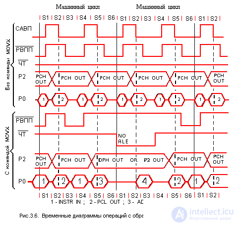
The main function of the CELP signal is to provide time coordination of the transfer from port 0 to the outer register of the low byte of the address in the read cycle from the runway. The signal to SAWP acquires the value 1 twice in each machine cycle. This happens even when there is no access to the runway in the sample cycle. Access to the VAP is possible only if the signal SAWP is absent. The first SAWP signal in the second machine cycle of the MOVX command is blocked. Consequently, in any MK-system that does not use the VAP, the SAWP signal is generated with a constant frequency equal to 1/16 of the resonator frequency, and can be used to synchronize external devices or to implement various time functions.
When accessing the RPP, the RPV signal is not generated, and when accessing the runway, it performs the function of a strobe signal reading. A complete cycle of reading the VFD, including the installation and removal of the THT signal, takes 12 periods of the resonator.
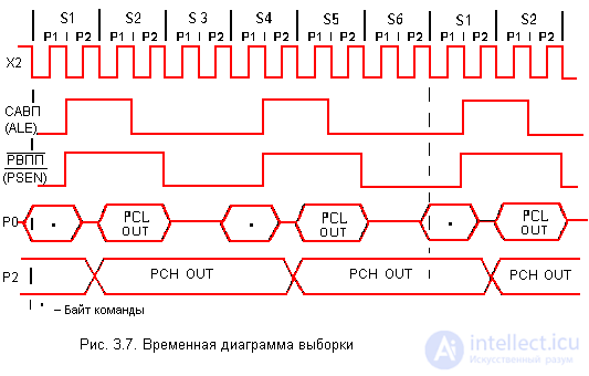
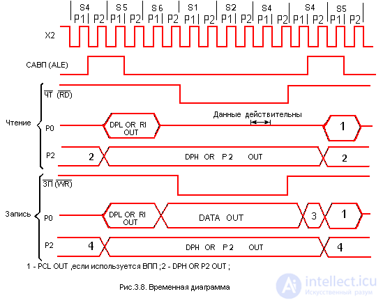
The timing diagrams in fig. 3.7 and fig. 3.8 illustrate the process of fetching a team from the runway and working with the PDD in read and write modes, respectively.
Special operation mode MK51. The contents of the MK51 program memory are filled once during the development of the MK-system and cannot be modified in the completed (final) product. For this reason, microcontrollers are not machines of the classic "von Neumann" architecture. RAM data (resident or external) can not be used to store program codes, as in MK, the command is sampled only from the area of program memory addresses. This feature of the MK architecture is explained by the fact that in most MK applications it is necessary to have one unchangeable application program stored in ROM, small capacity RAM for temporary storage of variables and effective, and therefore different methods of addressing program memory and data memory.
However, at the stage of development and debugging of application programs, the Von-Neumann type machine is very convenient, since it allows the developer to quickly change the codes of the application program placed in the RAM. С этой целью МК-система может быть модифицирована для совмещения адресного пространства ВПП и ВПД путем подключения внешней логики, как показано на рис. 3.9 .
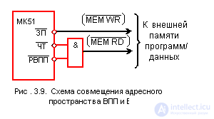
Здесь на выходе схемы И формируется строб-сигнал чтения, который может быть использован для объединения памяти программ и памяти данных во внешнем ОЗУ. При этом необходимо учитывать, что в МК51 на схемном уровне реализуются пять различных и независимых механизмов адресации для доступа к ПРР, РПД, ВПП, ВПД и блоку регистров специальных функций. Вследствие этого перемещаемая версия прикладной программы, которая отлаживается в среде внешней памяти программ/данных, будет отличаться от загружаемой в РП (окончательной) версии программы.
Подобный способ организации управления внешней памятью может быть использован в тех применениях МК51, где требуется оперативная перезагрузка или модификация прикладных программ (с помощью УВВ), как в ЭВМ классической архитектуры.
Два программируемых 16-битных таймера/счетчика (T/C0 и T/C1) могут быть использованы в качестве таймеров или счетчиков внешних событий. При работе в качестве таймера содержимое T/C инкрементируется в каждом машинном цикле, т.е. через каждые 12 периодов резонатора. При работе в качестве счетчика содержимое Т/С инкрементируется под воздействием перехода из 1 в 0 внешнего входного сигнал; подаваемого на соответствующий (T0, T1) вывод МК51. Опрос значения внешнего входного сигнала выполняется в момент времени S5P2 каждого машинного цикла. Содержимое счетчика будет увеличено на 1 в том случае, если в предыдущем цикле был считан входной сигнал высокого уровня (1), а в следующем _ сигнал низкого уровня (0). Новое (инкрементированное) значение счетчика будет сформировано в момент S3P1 в цикле, следующем за тем, в котором был обнаружен переход сигнала из 1 в 0. Так как на распознавание перехода требуется два машинных цикла, то максимальная частота подсчета входных сигналов равна 1/24 частоты резонатора. На длительность периода входных сигналов ограничений сверху нет. Для гарантированного прочтения входного считаемого сигнала он должен удерживать значение 1 как минимум течение одного машинного цикла МК51.
Для управления режимами работы T/C и для организации взаимодействия таймеров с системой прерывания используются два регистра специальных функций (РРТС и РУСТ), описание которых приводите в табл. 10.1 и табл. 10.2 соответственно. Как следует из описания управляющих бит РРТС, для обоих T/C режимы работы 0, 1 и 2 одинаковы. Режимы для T/C0 и T/C1 различны. Рассмотрим кратко работу T/C во всех четырех режимах.
Таблица 10.1. Регистр режима работы таймера/счетчика
Symbol | Позиция | Имя и назначение | ||
| GATE | TMOD.7 для T/C1 и TMOD.3 для T/C0 | Управление блокировкой. Если бит установлен, то таймер/счетчик " x " разрешен до тех пор, пока на входе "INTx " высокий уровень и бит управления " TRx" установлен. Если бит сброшен то Т/С разрешается, как только бит управления "TRx" устанавливается | ||
| C/ м T | TMOD.6 для T/C1 и TMOD.2 для T/C0 | Бит выбора режима таймера или счетчика событий. Если бит сброшен, то работает таймер от внутреннего источника сигналов синхронизации. Если бит установлен, то работает счетчик от внешних сигналов на входе "Тх" | ||
| M1 | TMOD.5 для T/C1 и TMOD.1 для T/C0 | Режим работы (см . примечание ) | ||
| M0 | TMOD.4 для T/C1 и TMOD.0 для T/C0 | |||
| Note | ||||
| M1 | M0 | Режим работы | ||
| 0 | 0 | Таймер МК48. "TLx" работает как 5 - битный предделитель | ||
| 0 | one | 16-битный таймер/счетчик. "ТНх" и "TLx" включены последовательно | ||
| one | 0 | 8-битный автоперезагружаемый таймер/счетчик . "ТНх" хранит значение, которое должно быть перезагружено в "TLx" каждый раз по переполнению | ||
| one | one | Таймер/счетчик 1 останавливается. Таймер/счетчик 0 : TL0 работает как 8-битный таймер/счетчик, и его режим определяется управляющими битами таймера 0. ТН 0 работает только как 8-битный таймер, и его режим определяется управляющими битами таймера 1 | ||
Таблица 10.2. Регистр управления/статуса таймера
Symbol | Позиция | Имя и назначение |
| TF1 | TCON.7 | Флаг переполнения таймера 1. Устанавливается аппаратурно при переполнении таймера/счетчика. Сбрасывается при обслуживании прерывания аппаратурно |
| TR1 | TCON.6 | Бит управления таймера 1 . Устанавливается/сбрасывается программой для пуска/останова |
| TF0 | TCON.5 | Флаг переполнения таймера 0. Устанавливается аппаратурно. Сбрасывается при обслуживании прерывания |
| TR0 | TCON.4 | Бит управления таймера 0. Устанавливается/сбрасывается программой для пуска/останова таймера/счетчика |
| IE1 | TCON.3 | Флаг фронта прерывания 1. Устанавливается аппаратурно, когда детектируется срез внешнего сигнала м ЗПР 1 ( м INT1 ). Сбрасывается при обслуживании прерывания |
| IT1 | TCON.2 | Бит управления типом прерывания 1. Устанавливается/сбрасывается программно для спецификации запроса м ЗПР1 (срез/низкий уровень) |
| IE0 | TCON.1 | Флаг фронта прерывания 0. Устанавливается по срезу сигнала м ЗПР 0 . Сбрасывается при обслуживании прерывания |
| IT0 | TCON.0 | Бит управления типом прерывания 0. Устанавливается / сбрасывается программно для спецификации запроса м ЗПР 0 (срез/низкий уровень) |
Режим 0. Перевод любого Т/С в режим 0 делает его похожим на таймер МК48 (8-битный счетчик), на вход которого подключен 5-битный предделитель частоты на 32. Работу Т/C в режиме 0 на примере Т/C1 иллюстрирует рис. 3.10,а . В этом режиме таймерный регистр имеет разрядность 13 бит. При переходе из состояния "все единицы" в состояние "все нули" устанавливается флаг прерывания от таймера TF1. Входной синхросигнал таймера 1 разрешен (поступает на вход T/C), когда управляющий бит TR1 установлен в 1 и либо управляющий бит GATE (блокировка) равен 0, либо на внешний вывод запроса прерывания м INT1 поступает уровень 1.
Отметим попутно, что установка бита GATE в 1 позволяет использовать таймер для измерения длительности импульсного сигнала, подаваемого на вход запроса прерывания.
Режим 1. Работа любого Т/С в режиме 1 такая же, как и в режиме 0, за исключением того, что таймерный регистр имеет разрядность 16 бит.
Режим 2. В режиме 2 работа организована таким образом, что переполнение (переход из состояния "все единицы" в состояние "все нули") 8-битного счетчика TL1 приводит не только к установке флага TF1 ( рис. 3.10,б ), но и автоматически перезагружает в TL1 содержимое старшего байта (TH1) таймерного регистра, которое предварительно было задано программным путем. Перезагрузка оставляет содержимое ТН1 неизменным. В режиме 2 Т/С0 и Т/С1 работают совершенно одинаково.
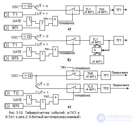
Режим 3. В режиме 3 Т/C0 и Т/C1 работают по разному. Т/C1 сохраняет неизменным свое текущее содержимое. Иными словами, эффект такой же, как и при сбросе управляющего бита TRI в нуль.
Работу T/C0 в режиме 3 иллюстрирует рис. 3.10,в . В режиме 3 TL0 и ТН0 функционируют как два независимых 8-битных счетчика. Работу TL0 определяют управляющие биты T/C0 (C/ м T, GATE, TR0), входной сигнал м INT0 и флаг переполнения TF0, Работу TH0, который может выполнять только функции таймера (подсчет машинных циклов МК), определяет управляющий бит TR1. При этом ТН0 использует флаг переполнения TF1.
Режим 3 используется в тех случаях применения МК51, когда требуется наличие дополнительного 8-битного таймера или счетчика событий. Можно считать, что в режиме 3 МК51 имеет в своем составе три таймера/счетчика. В том случае, если Т/С0 используется в режиме 3, Т/С1 может быть или включен, или выключен, или переведен в свой собственный режим 3, или может быть использован последовательным портом в качестве генератора частоты передачи, или, наконец, может быть использован в любом применении, не требующем прерывания.
Через универсальный асинхронный приемопередатчик (УАПП) осуществляется прием и передача информации, представленной последовательным кодом (младшими битами вперед), в полном дуплексном режиме обмена. В состав УАПП, называемого часто последовательным портом, входят принимающий и передающий сдвигающие регистры, а также специальный буферный регистр (SBUF) приемопередатчика. Запись байта в буфер приводит к автоматической переписи байта в сдвигающий регистр передатчика и инициирует начало передачи байта. Наличие буферного регистра приемника позволяет совмещать операцию чтения ранее принятого байта с приемом очередного байта. Если к моменту окончания приема байта предыдущий байт не был считан из SBUF, то он будет потерян.
Последовательный порт МК51 может работать в четырех различных режимах.
Режим 0. В этом режиме информация и передается и принимается через внешний вывод входа приемника (RXD). Принимаются или передаются 8 бит данных. Через внешний вывод выхода передатчика (TXD) выдаются импульсы сдвига, которые сопровождают каждый бит. Частота передачи бита информации равна 1/12 частоты резонатора.
Режим 1. В этом режиме передаются через TXD или принимаются из RXD 10 бит информации: старт-бит (0), 8 бит данных и стоп-бит (1). Скорость приема/передачи - величина переменная и задается таймером.
Режим 2. В этом режиме через TXD передаются или из RXD принимаются 11 бит информации: старт-бит, 8 бит данных, программируемый девятый бит и стоп-бит. При передаче девятый бит данных может принимать значение 0 или 1, или, например, для повышения достоверности передачи путем контроля по четности в него может быть помещено значение признака паритета из слова состояния программы (PSW.0). Частота приема/передачи выбирается программой и может быть равна либо 1/32, либо 1/64 частоты резонатора в зависимости от управляющего бита SMOD.
Режим 3. Режим 3 совпадает с режимом 2 во всех деталях, за исключением частоты приема/передачи, которая является величиной переменной и задается таймером.
Управление режимом работы УАПП осуществляется через специальный регистр с символическим именем SCON. Этот регистр содержит не только управляющие биты, определяющие режим работы последовательного порта, но и девятый бит принимаемых или передаваемых данных (RB8 и ТВ8) и биты прерывания приемопередатчика (RI и ТI).
Функциональное назначение бит регистра управления/статуса УАПП приводится в табл. 11.1 .
Прикладная программа путем загрузки в старшие биты спецрегистра SCON 2-битного кода определяет режим работы УАПП. Во всех четырех режимах работы передача из УАПП инициируется любой командой, в которой буферный регистр SBUF указан как получатель байта. Прием в УАПП в режиме 0 осуществляется при условии, что RI = 0 и REN = 1. В режимах 1, 2, 3 прием начинается с приходом старт-бита, если REN = 1.
В бите ТВ8 программно устанавливается значение девятого бита данных, который будет передан в режиме 2 или 3. В бите RB8 фиксируется в режимах 2 и 3 девятый принимаемый бит данных. В режиме 1, если SM2 = 0, в бит RB8 заносится стоп-бит. В режиме 0 бит RB8 не используется.
Флаг прерывания передатчика ТI устанавливается аппаратурно в конце периода передачи восьмого бита данных в режиме 0 и в начале периода передачи стол-бита в режимах 1,2 и 3. Соответствующая подпрограмма обслуживания прерывания должна сбрасывать бит ТI.
Флаг прерывания приемника RI устанавливается аппаратурно в конце периода приема восьмого бита данных в режиме 0 и в середине периода приема стоп-бита в режимах 1, 2 и 3. Подпрограмма обслуживания прерывания должна сбрасывать бит RI.
Таблица 11.1. Регистр управления/статуса УАПП
Symbol | Позиция | Имя и назначение | ||
| SM0 | SCON.7 | Биты управления режимом работы УАПП. Устанавливаются/ сбрасываются программно (см. примечание) | ||
| SM1 | SCON.6 | |||
| SM2 | SCON.5 | Бит управления режимом УАПП. Устанавливается программно для запрета приема сообщения, в котором девятый бит имеет значение 0 | ||
| REN | SCON.4 | Бит разрешения приема. Устанавливается/сбрасывается программно для разрешения/запрета приема последовательных данных | ||
| TB8 | SCON.3 | Передача бита 8. Устанавливается/сбрасывается программно для задания девятого передаваемого бита в режиме УАПП-9 бит | ||
| RB8 | SCON.2 | Прием бита 8. Устанавливается/сбрасывается аппаратурно для фиксации девятого принимаемого бита в режиме УАПП-9 бит | ||
| TI | SCON.1 | Флаг прерывания передатчика. Устанавливается аппаратурно при окончании передачи байта. Сбрасывается программно после обслуживания прерывания | ||
| RI | SCON.0 | Флаг прерывания приемника. Устанавливается аппаратурно при приеме байта. Сбрасывается программно после обслуживания прерывания | ||
| Note | ||||
| SM0 | SM1 | Режим работы УАПП | ||
| 0 | 0 | Сдвигающий регистр расширения ввода/вывода | ||
| 0 | one | УАПП-8 бит. Изменяемая скорость передачи | ||
| one | 0 | УАПП-9 бит. Фиксированная скорость передачи | ||
| one | one | УАПП-9 бит. Изменяемая скорость передачи | ||
В системах децентрализованного управления, которые используются для управления и регулирования в топологически распределенных объектах (например, прокатных станах, электроподвижном составе железных дорог и метрополитена, сборочных конвейерах и линиях гибких автоматизированных производств), возникает задача обмена информацией между множеством микроконтроллеров, объединенных в локальную вычислительно-управляющую сеть. Как правило, локальные сети на основе МК51 имеют магистральную архитектуру с разделяемым моноканалом (коаксиальный кабель, витая пара, оптическое волокно), по которому осуществляется обмен информацией между МК.
В регистре специальных функций SCON микроконтроллера имеется управляющий бит SM2, который в режимах 2 и 3 УАПП позволяет относительно простыми средствами реализовать межконтроллерный обмен информацией в локальных управляющих сетях.
Механизм межконтроллерного обмена информацией через последовательный порт МК51 построен на том, что в режимах 2 и 3 программируемый девятый бит данных при приеме фиксируется в бите RB8. УАПП может быть запрограммирован таким образом, что при получении стоп-бита прерывание от приемника будет возможно только при условии RB8 = 1. Это выполняется установкой управляющего бита SM2 в регистре SCON.
Поясним процесс межконтроллерного обмена информацией на примере. Пусть ведущему МК требуется передать блок данных некоторому (или нескольким) ведомому МК. С этой целью ведущий МК в протокольном режиме "широковещательной" передачи (всем ведомым МК) выдает в моноканал байт-идентификатор абонента (код адреса МК-получателя), который отличается от байтов данных только тем, что в его девятом бите содержится 1. Программа реализации протокола сетевого обмена информацией должна быть построена таким образом, чтобы при получении Райта- идентификатора (RB8 = 1) во всех ведомых МК произошли прерывание прикладных программ и вызов подпрограммы сравнения байта-идентификатора с кодом собственного сетевого адреса. Адресуемый МК сбрасывает свой управляющий бит SM2 и готовится к приему блока данных. Остальные ведомые МК, адрес которых не совпал с кодом байта-идентификатора, оставляют неизменным состояние SM2 = 1 и передают управление основной программе. При SM2 = 1 ин формационные байты, передаваемые по моноканалу и поступающие в УАПП ведомых МК, прерывания не вызывают, т.е. игнорируются.
В режиме 1 УАПП автономного МК управляющий бит SM2 используется для контроля истинности стоп-бита (при SM2 = 1 прерывание не произойдет до тех пор, пока не будет получено истинное (единичное) значение стоп- бита). В режиме 0 бит SM2 не используется и должен быть сброшен.
Скорость приема/передачи, т.е. частота работы УАПП в различных режимах, определяется различными способами.
В режиме 0 частота передачи зависит только от резонансной частоты кварцевого резонатора f0 = f рез /12. За один машинный цикл последовательный порт передает один бит информации.
В режимах 1, 2 и 3 скорость приема/передачи зависит от значения управляющего бита SMOD в регистре специальных функций РУМ ( табл. 11.2 ).
В режиме 2 частота передачи определяется выражением f 2 = (2 MOD /64)*f рез иными словами, при SMOD = 0 частота передачи равна (1/64) *f рез , а при SMOD = 1 равна (1/32)*f рез .
Таблица 11.2. Регистр управления мощностью РУМ
Symbol | Позиция | Имя и назначение |
| SMOD | PCON.7 | Удвоенная скорость передачи. Если бит установлен в 1, то скорость передачи вдвое больше, чем при SMOD = 0 |
| ---- | PCON.6 | Не используются |
| ---- | PCON.5 | |
| ---- | PCON.4 | |
| GF1 | PCON.3 | Флаги, специфицируемые пользователем (флаги общего назначения) |
| GF0 | PCON.2 | |
| PD | PCON.1 | Бит пониженной мощности. При установке бит а в 1 МК переходит в режим пониженной потребляемой мощности |
| IDL | PCON.0 | Бит холостого хода. Если бит установлен в 1, то МК переходит в режим холостого хода |
| Note. При одновременной записи 1 в PD и IDL бит PD имеет преимущество. Сброс содержимого РУМ выполняется путем загрузки в него кода 0XXX0000. | ||
В режимах 1 и 3 в формировании частоты передачи кроме управляющего бита SMOD принимает участие таймер 1. При этом частота передачи зависит от частоты переполнения (OVT1) и определяется следующим образом:
f 1, 3 = (2 SMOD /32)*f OVT1 .
Прерывание от таймера 1 в этом случае должно быть заблокировано. Сам T/C1 может работать и как таймер, и как счетчик событий в любом из трех режимов. Однако наиболее удобно использовать режим таймера с автоперезагрузкой (старшая тетрада TMOD = 0010В). При этом частота передачи определяется выражением:
f 1, 3 = (2 SMOD /32)*(f рез /12)/(256-(TH1))
В табл. 11.3 приводится описание способов настройки Т/С1 для получения типовых частот передачи данных через УАПП.
Таблица 11.3. Настройка таймера 1 для управления частотой работы УАПП
Частота приема/передачи (BAUD RATE) | Частота резонатора, МГц | SMOD | Таймер/счетчик 1 | ||
C/T | Режим (MODE) | Перезагружаемое число | |||
| Режим 0, макс: 1 МГц | 12 | X | X | X | X |
| Режим 2, макс: 375 кГц | 12 | one | X | X | X |
| Режимы 1, 3: 62.5 кГц | 12 | one | 0 | 2 | 0FFH |
| 19.2 кГц | 11.059 | one | 0 | 2 | 0FDH |
| 9.6 кГц | 11.059 | 0 | 0 | 2 | 0FDH |
| 4.8 кГц | 11.059 | 0 | 0 | 2 | 0FAH |
| 2.4 кГц | 11.059 | 0 | 0 | 2 | 0F4H |
| 1.2 кГц | 11.059 | 0 | 0 | 2 | 0E8H |
| 137.5 Гц | 11.059 | 0 | 0 | 2 | 1DH |
| 110 Гц | 6 | 0 | 0 | 2 | 72H |
| 110 Гц | 12 | 0 | 0 | one | 0FEEBH |
Режим 0. На рис. 3.11 показаны упрощенная структурная схема УАПП и временная диаграмма его работы в режиме 0. Данные передаются и принимаются через вывод RXD. Через вывод TXD выдаются синхросигналы сдвига.
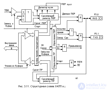
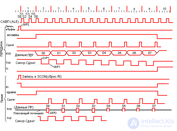
Transmission starts with any command that sends a data byte to the SBUF. At time S6P2, the MK51 control device, using a signal, writes to the buffer, writes a byte to the shift register of the transmitter, sets the trigger for the ninth bit, and starts the transmission control unit, which, after one machine cycle, generates the enabling signal Send . At the same time, at the time of S6P2 of each machine cycle, the content of the shift register is shifted to the right (by forward bits) and fed to the RXD pin. Zeros are written to the higher bits of the shift register of the transmitter. When a zero signal is received from the detector, the Transmitter is empty . The transmitter control unit removes the Send signal and sets the TI flag (S1P1 time of the tenth machine cycle after the receipt of a signal. Write to the buffer) .
Reception begins when REN = 1 and RI = 0. At the time of S6P2 of the next machine cycle, the receiver control unit generates an enable signal Receipt on which shift clock signals are transmitted to the TXD output and data bit values that are read from the RXD input begin to be generated at the receiver shift register at times S5P2 each machine cycle. At the time S1P1 of the tenth machine cycle after the signal. Writing to SCON , the receiver control unit overwrites the contents of the shift register to the buffer, removes the enabling signal Receive and sets the RI flag.
Mode 1. In fig. 3.12 the block diagram is shown ( Fig. 3.12, a ) and the time diagrams of the UART operation in receiving and transmitting data ( Fig. 3.12, b, c ). Through the TXD pin, the UART transmits, and from the RXD pin, it receives 10 bits: start bit (0), 8 data bits and stop bit (1). Upon receipt, the stop bit enters the RB8 bit of the SCON register.
A transfer is initiated by any command in which the byte receiver is the SBUF register. The control signal generated at the same time. Writing to the buffer loads 1 into the ninth bit of the shift register of the transmitter, starts the transmission control unit and at time S1P1 generates the enabling signal Send. This signal sends a start-bit to the TXD pin, and then (according to the Data enable signal) data bits. Each bit transmission period is equal to 16 clocks of the internal counter.
Reception begins when a signal is detected at the RXD input from state 1 to state 0. For this, under the control of an internal counter, the RXD input is polled 16 times during the bit representation period. As soon as the transition from 1 to 0 at the RXD input is detected, the 1FFH code is loaded into the shift register of the receiver, the internal modulo-16 counter is immediately reset and restarted to align its transitions with the representation period bits of the received bits. Thus, each submission period of a bit is divided into 16 periods of an internal counter. In states 7, 8 and 9 of the counter, in each period of the bit representation, a signal is polled at the RXD input. The read value of the received bit is the one that was received at least twice from three measurements (majority voting on the principle “two out of three”). If the value received in the first cycle is not equal to 0, the reception control unit returns to searching for a transition from 1 to 0. This mechanism suppresses false (failed) start-bits. The true start-bit is shifted in the register of the receiver, and the reception of the remaining bits of the parcel continues. The reception control block will generate a buffer load signal, set RB8 and RI flag only if two conditions are satisfied during the last shift cycle: bit RI = 0, and either SM2 = 0, or the received stop bit is 1. If one of these If two conditions are not met, the received bit sequence is lost. At this time, regardless of whether the specified conditions are met or not, the reception control unit again begins to search for a transition from 1 to 0 at the input of the RXD.
Modes 2, 3. Through the TXD pin, the UART transmits or receives 11 bits from the RXD pin: start bit (0), 8 data bits, programmable ninth bit and stop bit (1). The timing diagram ( Fig. 3.12, c ) shows the operation of the UART when transmitting and receiving data in modes 2 and 3. As can be seen, modes 2 and 3 differ from mode 1 only in the presence of the ninth programmable bit. As a result, the end of the receive cycle conditions change somewhat: the receiver control unit will generate a control signal. Load the buffer, load RB8 and set the RI flag only if two conditions are met during the last shift cycle: bit RI = 0 and either SM2 = 0 or value The ninth data bit received is 1.
A simplified interrupt scheme MK51 is shown in Fig. 3.13 .
External interrupts m INT0 and m INT1 can be caused either by a level or by a signal transition from 1 to 0 at the inputs of the MK51, depending on the values of the control bits IT0 and IT1 in the TCON register. From external interrupts, the IE0 and IE1 flags are set in the TCON register, which initiates a call to the corresponding interrupt service routine. The reset of these flags is performed hardware only if the interruption was triggered by a signal transition (slice). If the interruption is caused by the input signal level, then the corresponding interrupt service routine controls the IE flag by affecting the interrupt source to clear the request.
The interrupt request flags from the TF0 and TF1 timers are automatically cleared when the control is transferred to the maintenance routine. The interrupt request flags RI and TI are set by the UART control unit hardware, but must be reset by the program.
Interrupts can be caused or canceled by the program, since all the listed flags are program-accessible and can be set / cleared by the program with the same result as if they were set / cleared by hardware.
In the special function register block there are two registers designed to control the interrupt mode and priority levels. The formats of these registers with the symbolic names IE and IP are described in Table. 12.1 and table. 12.2, respectively. The ability to programmatically set / reset any control bit in these two registers makes the MK51 interrupt system extremely flexible.
Table 12.1. Interrupt Mask Register (RMP)
Symbol | Position | Name and Purpose |
| EA | IE.7 | Unlocking interrupts. Cleared by software to disable all interrupts, regardless of the state of IE4 - IE0 |
| ---- | IE.6 | Not used |
| ---- | IE.5 | |
| ES | IE.4 | UART interrupt enable bit. Setup / Reset by the program to enable / disable interrupts from TI or RI flags |
| ET1 | IE.3 | Timer Interrupt Enable Bit 1. Set / reset by the program to enable / disable timer 1 interrupts |
| EX1 | IE.2 | Enable external interrupt enable bit 1. Set / reset by the program to enable / disable interrupts |
| ET0 | IE.1 | Timer 0 interrupt enable bit. Works the same as IE.3. |
| EX0 | IE.0 | Enable external interrupt 0 bit. Works the same as IE.2. |
Table 12.2. Interrupt Priority Register
Symbol | Position | Name and Purpose |
| ---- | IP.7 - IP.5 | Not used |
| PS | IP.4 | Bit priority UART. Setup / Reset by the program for assigning a UART interrupt of higher / lower priority |
| PT1 | IP.3 | Timer 1 priority bit. Set / reset by the program for assigning an interrupt from timer 1 to the highest / lowest priority |
| PX1 | IP.2 | External Interrupt Priority Bit 1. Set / reset by the program for assigning high / low priority to external interrupt m INT1 |
| PT0 | IP.1 | Timer 0 priority bit. Works the same as IP.3. |
| PX0 | IP.0 | The external interrupt priority bit is 0. It works similarly to IP.2 |
Interrupt flags are polled at the time of S5P2 of each machine cycle. Priority interrupt ranking is performed during the next machine cycle. The interrupt system will form a hardware call (LCALL) of the corresponding maintenance routine, if it is not blocked by one of the following conditions:
1) an interrupt request of an equal or higher priority level is being serviced;
2) the current machine cycle _ is not the last in the cycle of the command being executed;
3) a RETI command is executed, or any command related to accessing the IE or IP registers.
Note that if the interrupt flag was set, but according to one of the above conditions did not receive service, and by the time the lock was completed it was cleared, then the interrupt request is lost and is not remembered anywhere.
According to the hardware-generated LCALL code, the interrupt system pushes onto the stack only the contents of the command counter (PC) and loads the address of the vector of the corresponding service subroutine into the command counter. The vector of unconditional control transfer (JMP) to the starting address of the interrupt service routine must be located at the vector address. The maintenance routine should, if necessary, begin with writing to the stack (PUSH) of a program status (PSW) dispute, battery, expander, data pointer, etc. and end with recovery commands from the stack (POP). The interrupt service subroutines are necessarily terminated by the RETI command, by which the saved return address to the main program is reloaded from the stack to the command counter. The RET command also returns control to the interrupted main program, but it does not release the interrupt blocking, which makes it necessary to have a software mechanism for analyzing the end of the maintenance procedure for this interrupt.
Under the influence of external electrical signals, the MK51 can be electrically programmed or, in other words, the object codes of the application program can be loaded into the PPP of the microcontroller. The contents of the RPP microcontroller can be destroyed by exposure to an ultraviolet light source (erasing) for subsequent reprogramming. The microcontroller has a means of protection against software “robbery”, which makes it impossible to read the contents of the RPP in the final product and, consequently, preserve the professional secrets of the developer of the application software.
Download programs in RPP. In programming mode, the MK51 should operate at a lower frequency (with a 4-6 MHz resonator) due to the need for multiplexing address and code information on the internal bus. In fig. 3.14 shows the connection diagram of the MK51 to the programmer.

The cell address of the PPP, into which the application program byte is to be loaded, is fed to the pins of port 1 and the P2.0-P2.3 ports of port 2. At the same time, the loaded byte enters the MC via port 0. Conclusions P2.4-P2.6 and meters PSEN must be grounded, and the P2.7 and RST terminals must be supplied with a logic level 1 (for the RST input the logic 1 level is at least 2.5 V, for the remaining inputs the standard TTL level). At the EA / VPP input, the +5 V level is maintained, but at the moment of loading the byte, it must be connected to a voltage source with a +21 V. At this time, the level at the ALE / m PROG input should be reset to at least 50 ms 0. After that, the voltage at the EA / VPP input returns to the +5 V level. The +21 V voltage source (VPP) must be very well stabilized, since exceeding the +21.5 V limit value at the EA / VPP input leads to irreversible damage. RPP.
Record bit protection. The RPP security bit, when set, prohibits access to the RPF by any external means. The write scheme of the protection bit is shown in fig. 3.15 .

The procedure for writing the protection bit is the same as when loading programs into the FAR, but the P2.6 pin should be supplied with level 1. Signals at the ports of ports P0, P1 and P2.0-P2.3 can be in any state. Once set, the protection bit can be reset only by completely erasing the FAR under the source of UV radiation.
Verification of programs. If the protection bit is not programmed, then the contents of the PDP can be read to verify the correctness of the application program loading either during the programming or after the end of the MK51 programming. Access to the PDP cells ( Fig. 3.16 ) is carried out in the same way as when programming the PDP, except that signal 0 is sent to pin P2.7, used as a read strobe signal. The read command codes and the corresponding RPD addresses can be displayed for visual control on any external indicator and, in addition, can be transferred to the RAM of the instrumental computer for disassembling.
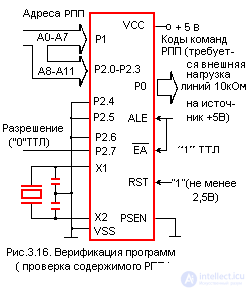
Erasing RPP. To erase the contents of the RPP, the microcontroller should be placed under a source of UV radiation with a wavelength less than 4 * 10 -7 m. If a quartz lamp has a light power of 12000 mW / cm 2 , and the distance between the light source and the MC is 2-3 cm, then the exposure 20-30 minutes provides a light dose sufficient for reliable erasure of the PSC. After deleting, the unit contains all units.
Since the spectrum of sunlight and luminescent illumination contains radiation with a wavelength less than 4 * 10 -7 m, the stay of the MK under the influence of these light sources longer than the established limit (about one week in the sunlight or about three years under fluorescent lighting) may result to distort the contents of the RPT. To protect the contents of the RPP from destruction under the influence of light on the window of the housing MK strengthen light-proof screen.
At the stage of debugging an application program in the prototype MK-system, the mode of step-by-step (command-based) program execution is very convenient for the developer. The MK51 interrupt system allows you to implement this mode of operation by using several additional commands. As described in the Interrupt System section, an external interrupt request will not be served as long as the interrupt is served with equal priority. This request will be accepted only after one command after the RETI command is executed. In other words, once having called an interrupt service routine, it is impossible to call it again until at least one command of the main program is executed. This property of the MK51 interrupt system can be used to implement the step-by-step mode as follows: one of the external interrupts, for example, INT0 (microcontroller pin P3.2), be programmed to present the request by the signal level (IT = 0), and the interrupt service routine must end with the sequence teams:
| Jnb | P3.2, $ | ; Waiting for Level 1 at INT0 |
| Jb | P3.2, $ | ; Waiting for level 0 at input INT1 |
| RETI | ; Return and execution of one command |
Here, the $ symbol denotes the current contents of the command counter. Now, if the INT0 pins give a signal from the STEP key of the debugging module of the system, then the MK51 will send the external interrupt 0 maintenance routine to the MK51 signal until it detects a new pulse at the INTO input (transition from 0 to 1 and again to 0). The RETI command will return to the main program, execute one command in it and immediately call the external interrupt 0 service subroutine.
Reset. Unlike the MK48, the MK51 is reset by applying the signal 1 to the SBR (RST) input. For a confident MK51 reset, this signal 1 must be held at the SBR input for at least two machine cycles (24 resonator periods). The quasi-two-sided buffer circuits of the external terminals ALE and m PSEN are in the input mode. The following registers are reset by the CBR signal: PC, ACC, B, PSW, DPTR, TMOD, TCON, T / C0, T / C1, IE, IP and SCON, only the high bit is reset in the PCON register, the stack pointer is loaded code 07H, and in ports P0-P3 - codes 0FFH. SBUF register state is undefined. The RRF signal does not affect the contents of the RPD cells. When power is turned on (VCC), the contents of the RPD are undefined, except for the operation of returning from low power mode.
In fig. 3.17 shows a diagram of the automatic generation of the signal to the SSR when power is turned on. The time required for a full charge of the tank ensures that the resonator starts up and works for more than two machine cycles.
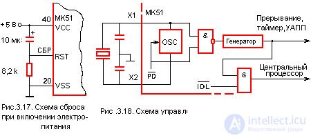
Idle mode. Any command that sets the IDL control bit (PCON.0) in the power control register will switch the MK51 to idle mode. At the same time, the internal clock signal generator continues to work ( Fig. 3.18 ). All registers retain their value. On the findings of all ports, the logical state that was on them at the moment of transition to the idle mode is kept. On pins ALE and m PSEN level 1 is formed.
Exit idle mode can be either by a signal to the SBR, or by interruption. Any of the allowed interrupt signals will lead to hardware reset of the PCON.0 bit and thereby terminate the idle mode. After the execution of the RETI command (exit from the interrupt service routine), the command that follows the program after the command that has switched MK51 to idle mode will be executed. (In some versions of the MK51 this mode may be absent.)
Low Power Mode. В тех применениях МК-систем, где потребление электроэнергии, а следовательно, габаритные размеры и масса источника электропитания являются одними из основных показателей качества изделия, возможно использование МК51 в режиме пониженного энергопотребления. Перевод МК51 в этот режим возможен по команде, которая установит бит PCON.1 в регистре управления мощностью (см. табл. 11.2 ). В этом режиме останавливается генератор синхросигналов, содержимое РПД и регистров специальных функций сохраняется, а на выходных контактах портов удерживаются значения, соответствующие содержимому их буферных регистров. Выходы сигналов ALE и м PSEN сбрасываются. При этом электропитание осуществляется через вывод RST/VPD.
В режиме пониженного энергопотребления напряжение электропитания (VCC) может быть отключено. Перед выходом из режима оно должно быть восстановлено до номинального значения.
Выход из режима пониженного энергопотребления возможен только по сигналу RST. При этом переопределяются все регистры специальных функций, но содержимое РПД не изменяется. (В некоторых модификациях МК51 этот режим может отсутствовать.)
Защита от падения напряжения. При не мгновенных отказах блока электропитания МК-системы можно обеспечить сохранность содержимого РПД с помощью маломощного (батарейного) аварийного источника электропитания, подсоединяемого к выводу RST/VPD. Для этого МК при получении сообщения о грозящем падении напряжения VCC (прерывание от системы контроля электропитания) должен перегрузить в РПД основные параметры прерванного процесса и выдать сигнал, разрешающий подключение к выводу RST/VPD аварийного источника питания. Все эти процедуры МК должен успеть выполнить до того, как напряжение основного источника электропитания упадет ниже рабочего предела. После восстановления номинального значения напряжения в основной цепи электропитания выполняется системный сброс, и источник аварийного электропитания может быть отключен.
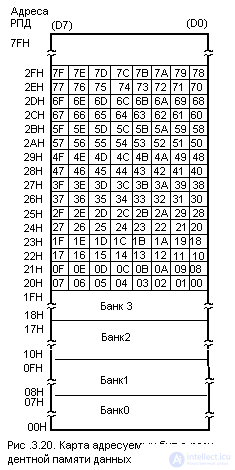
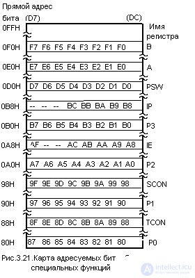

Comments
To leave a comment
Digital devices. Microprocessors and microcontrollers. computer operating principles
Terms: Digital devices. Microprocessors and microcontrollers. computer operating principles