Lecture
Abstract: The main elements that make up the system of logic elements, their circuit design, static and dynamic parameters, the order of designing combinational circuits are considered using the example of a one-bit adder.
A system of logical elements is called a functionally complete set of logical elements united by common electrical, structural, and technological parameters and using the same type of inter-element connections [1]. The element systems contain elements for performing logical operations, memory elements, elements realizing the functions of computer nodes, as well as elements for amplifying, reconstructing, and generating signals of standard form.
The conditional-graphic symbols (UGO) of some logical elements are presented in Figure 13.1.
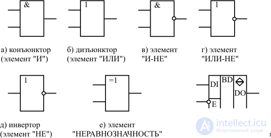
The HBO element is a rectangle to which the input signals fit on the left, and the output goes to the right. Inside the rectangle is a symbol of the logical function performed by the element. If the value of the output signal takes an inverse value with respect to the function indicated inside the element, then this output is indicated by a circle on the UHT of the element (Fig. 13.1, c - 13.1, d). Similarly, if the active level of the input signal is a logical "0", then this input is indicated by a circle (input E of element 13.1, g).
If an element performs a complex function, has several functionally different groups of inputs and outputs, then the inputs and outputs are separated from the main field of the UHEC by vertical lines. Inside each of the resulting fields, functionally different groups of inputs and outputs are separated from each other by horizontal lines. Fig. 13.1, g shows an element whose output can be in one of three states: logical "0", logical "1", high resistance state. In a state of high resistance, the output of an element is disconnected from the inputs of all other elements with which it is associated. The E input (enable) of this item controls the state of its output. Since on the conditional graphic designation this input is marked by a circle, it follows that the function of transmitting a binary signal from the input to the output of the element is performed in the logical state "0" at the resolution input E. If the input E is given a logical signal "1", the output of the element is in the disabled (the so-called "third") state.
Each logical element is an electronic technical product (Fig. 13.2). In these circuits, all transistors operate in a key mode. This means that when a high level signal is applied to the base of the transistor, its resistance becomes negligible, that is, the transistor seems to be “pulled to a point”. With a low potential at the base of the transistor, the resistance between the collector and the emitter becomes extremely large, which actually means breaking the circuit.
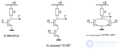
Consider this on the example of the inverter (Fig. 13.2, a). If the signal X has a high potential, then the key realized on the transistor is closed, and the potential of the point Y is low. Otherwise, the connection between point Y and the ground is broken, and the signal Y has a high level, which ensures the realization of the logical function "negation".
For the element "AND-NOT", the signal at point Y will have a low level (DL) only when both signals X1 and X2 have a high level (DL). The operation of this element is described in table 13.1.
| X 1 | X 2 | Y |
|---|---|---|
| WELL | WELL | WU |
| WELL | WU | WU |
| WU | WELL | WU |
| WU | WU | WELL |
If we take, as is done in the most common series of logical elements, a high signal level for a logical "1", and a low level for a logical "0", then we obtain the truth table of this element (table 13.2).
| X 1 | X 2 | Y |
|---|---|---|
| 0 | 0 | one |
| 0 | one | one |
| one | 0 | one |
| one | one | 0 |
This table corresponds to the logical function "AND-NOT."
At the same time, taking the high signal level as the logical "0", and the low level as the logical "1", we get the following truth table (Table 13.3).
| X 1 | X 2 | Y |
|---|---|---|
| one | one | 0 |
| one | 0 | 0 |
| 0 | one | 0 |
| 0 | 0 | one |
This table already corresponds to the OR-NOT function.
Thus, the coding of signals in the system of logical elements can influence the logical function performed by it. In the future we will assume the signal coding adopted for table. 13.2.
For the "OR-NOT" element (see Fig. 13.2), the signal at point Y will have a high level only when both signals X1 and X2 are low. The operation of this element is described in table. 13.4, and his truth table under the assumptions about the signal coding - table 13.5. This table corresponds to the logical function "OR-NOT."
| X 1 | X 2 | Y |
|---|---|---|
| WELL | WELL | WU |
| WELL | WU | WELL |
| WU | WELL | WELL |
| WU | WU | WELL |
| X 1 | X 2 | Y |
|---|---|---|
| 0 | 0 | one |
| 0 | one | 0 |
| one | 0 | 0 |
| one | one | 0 |
Parameters of elements can be divided into static and dynamic [1]. Static parameters are transient-invariant and are measured in a static mode. Dynamic, on the contrary, determine the reactive properties of the element and are measured during transients.
Static parameters include currents flowing at the terminals of the circuit and the corresponding voltages. Note among these parameters the following:
Among the numerous dynamic parameters characterizing the scheme, select the following:
We illustrate some static and dynamic parameters of logic circuits using the example of the “NO” element (see. Fig. 13.2, a). The time diagram of the input and output signals of this element, on which its static and dynamic parameters are marked, is shown in fig. 13.3.

When designing circuits that perform a particular logical function, it is necessary to ensure the minimization of hardware costs for the implementation of these circuits, and in many cases it is necessary to reduce the nomenclature of the used logical elements. The last requirement is implemented by selecting the appropriate system of elements. Currently, the main series of integrated logic circuits include elements that make up some functionally complete logical basis, as well as additional elements that implement frequently occurring logic functions [1]. As functionally complete bases, as a rule, singleton bases "AND-NO" or "OR-NO" are used.
Consider the design stages of combinational logic circuits on a single-element basis "AND-NOT" without using any additional logic elements on the example of designing a single-bit combinational adder. Such an adder is the basis for constructing a multi-digit summing circuit that performs operations on numbers represented in a particular code.
An example of performing the operation of summation of numbers represented in the reverse code:
X ok = 0.1011
Y OK = 1.0110
+ 0.1011
1.0110
+ 1.0.0001
_______one
0.0010
It is clear from the example that in each digit there is a summation of the corresponding bits of the operands and the transfer coming from the previous bit (for the lower bit, cyclic transfer from the sign bit). At the same time, the value of the sum in this digit and the transfer to the next digit are generated.
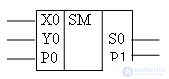
The conditional-graphic designation of the element performing these actions is shown in Fig. 13.4.
Consider the main stages of designing such a scheme .
Stage 1. Representation of the function performed by the projected circuit in canonical form, that is, in the form of a truth table or one of the perfect normal recording forms . Usually at this stage, the function is easier to describe the truth table. Since a two-output logic circuit is being designed, it is necessary to present a truth table for each of its outputs (Table 13.6).
| Inputs | Outputs | |||
|---|---|---|---|---|
| X i | Y i | PI | S i | Pi + 1 |
| 0 | 0 | 0 | 0 | 0 |
| 0 | 0 | one | one | 0 |
| 0 | one | 0 | one | 0 |
| 0 | one | one | 0 | one |
| one | 0 | 0 | one | 0 |
| one | 0 | one | 0 | one |
| one | one | 0 | 0 | one |
| one | one | one | one | one |
Stage 2. Minimization of the logical function . At this stage, you can use any minimization methods [5]. The specificity of minimizing multi-output functions is the need to obtain a device having a minimum overall equipment, that is, one function should be minimized, taking into account the possible use of a part of the equipment obtained to minimize another function. In our example, we will not consider this feature and carry out autonomous minimization of each function. The minimization of logical functions can be carried out by various methods: Quine's method, its modification - by Quine's method - McClasky, by the Veitch diagrams. The method of Veitch diagrams is conveniently used to minimize the functions of a small (up to four) number of variables. The Veitch diagram for the function S i is presented in Table. 13.7.
| y i | y i | |||
| x i | 0 | one | 0 | one |
| x i | one | 0 | one | 0 |
| p i | pi | p i | ||
It can be seen from the diagram that the minimum disjunctive normal form for the sum function of a one-bit adder coincides with its perfect disjunctive normal form:

The Veitch diagram for the function P i + 1 is presented in Table. 13.8.
| y i | y i | |||
| x i | one | one | one | 0 |
| x i | 0 | one | 0 | 0 |
| p i | pi | p i | ||
The minimum disjunctive normal form for this function is:

Stage 3. Transfer of the function to the basis in which the scheme will be built . In the chosen variant, this is the basis of the "Schaeffer Bar":
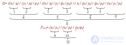
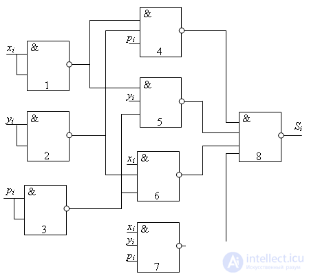
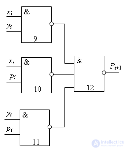
Stage 4. Drawing up a diagram on the elements that implement the functions of the selected basis . For a more visual display of this stage, the numbers of the elements that will implement one or another part of the function are indicated above. The resulting diagrams are presented in Figures 13.5 and 13.6.

Comments
To leave a comment
Digital devices. Microprocessors and microcontrollers. computer operating principles
Terms: Digital devices. Microprocessors and microcontrollers. computer operating principles