Lecture
It is known that the mathematical basis of digital computing devices is binary arithmetic, which uses only two numbers - 0 and 1. The choice of the binary number system was dictated by the requirements of simplicity of technical implementation of the most complex tasks using only one basic element - a key that has two states: on (closed) or off (open). If the first key state is taken as a conditional (logical) unit, then the second will reflect a conditional (logical) zero or vice versa. Possible combinations are shown in fig. 9.1, 9.2 and 9.3.
In fig. 9.1 shows the keys 1 and 0, controlled by the keys 1 and 0, respectively, and auxiliary devices in the form of a 5 V battery with an internal resistance of 100 Ohms and a 6 V incandescent lamp with a power of 30 mW, which make it possible to judge the state of the key: if it is in position 1, the llama burns (Fig. 9.1, a), or does not burn if it is in position 0 (Fig. 9.1, b).
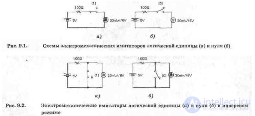
Perhaps a different arrangement of keys with respect to auxiliary devices, shown in Fig. 9.2. In these schemes, the state of indicators of zero or one is opposite to that shown in Fig. 9.1. When you press the key 1, the indicator fixes the state 0 (Fig. 9.2, a) and vice versa (Fig. 9.2, b). Consequently, the diagrams in Fig. 9.2 by the output signal (state of indicator lights) are inverse (inverse) with respect to the circuits in Fig. 9.1. Therefore, such keys are called inverters,
Since digital systems contain a huge number of keys (there are several millions of them in a single microprocessor) and they cannot communicate with each other about their status by blinking light bulbs, electrical voltage signals are used to exchange information. In this case, the keys, as a rule, are used in inverse mode in accordance with the schemes in Fig. 9.3,
In fig. 9.3 resistance 490 Ohm simulates the internal resistance of the key load (analog of collector resistance in the transistor key), resistance 10 Ohm - resistance of a closed electronic key, resistance 500 Ohm - resistance of an open key taking into account external load. As can be seen from fig. 9.3, the presence of a logical zero at the output (inversion 1) is indicated by a voltage of 100 mV (in practical constructions it can be more), and the presence of a logical unit by a voltage of 2.55 V (normalized to 2.4 V). Electronic keys are designed in such a way that, in the worst combinations of input and output parameters, the keys can distinguish between logical unit and zero signals.
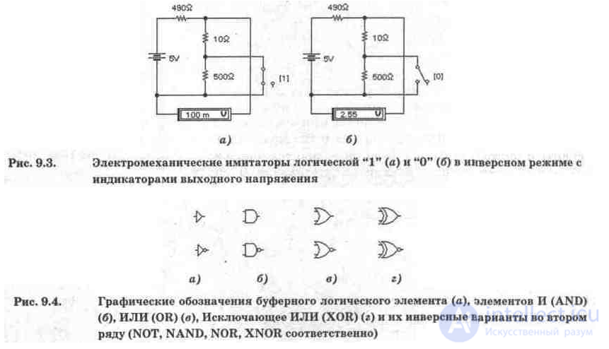
In digital technology, practical analogues of the circuits considered are called logical elements. In this case, depending on the functions performed, each element has its own name and corresponding graphic designation. In fig. 9.4 shows the designations of the basic logic elements adopted in the program EWB 4.1.
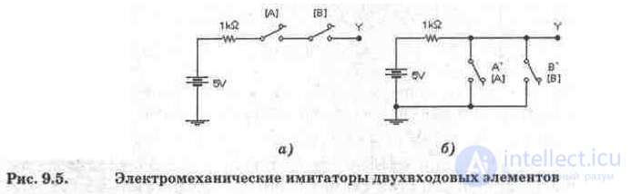
The electromechanical analogue of the buffer element is the simulators in Fig. 9.3, and the logical element NOT (NOT) - in Fig. 9.2 and 9.3. Electromechanical analogues of two-input elements AND, AND-NOT are shown in Fig. 9.5.
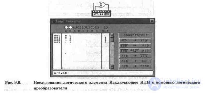
If the EWB program has such a wonderful tool as a logic converter, it is advisable to conduct research on logical circuits with its help. As an example in fig. 9.6 is a diagram for examining an XOR element.
The connection of the element under investigation to the logic converter is evident from Fig. 9.6. It is also obvious that with two inputs, only four combinations of input signals are possible, which is displayed on the screen of the converter in the form of a truth table, which is generated after pressing the key 
To get the Boolean expression of the element under study, press the key 
This expression is given on an additional display located at the bottom of the front panel in the form of two terms corresponding to the TRUE output signal (a logical unit signal at the OUT output). Comparison of the obtained expression with the truth table convinces us that there are really two such combinations, given that the following notation is used in the resulting expression: A '= 0 - inversion A = 1, TU = 0 - inversion B = 1, + sign logical operation OR.
Using a logic converter, you can conduct not only an analysis of logical devices, but also their synthesis. Suppose we need to draw up a circuit and a Boolean expression for a logical element for which the output combination in the truth table is not IT, as in Fig. 9.6, and 1101. To make the necessary changes, mark the character to be changed in the OUT column with the cursor, change it using the keyboard, and then, moving the column with the cursor keys, change the characters in other rows as necessary. After making all the changes, press the keys sequentially  and we get the result presented in Fig. 9.7. The synthesized logic device is shown in the upper left corner of Fig. 9.7, and its Boolean expression on the secondary display.
In a more general case, to perform the synthesis, it is advisable to proceed as follows. By clicking on the icon of the logic converter directly on the instrument line, we open its front panel. We activate the cursor of the terminal button A, B ... H (starting with A), the number of which is equal to the number of inputs of the synthesized device. We make the necessary changes to the OUT column and after pressing the control keys of the above control keys on the converter panel, we get the result in the form of a diagram on the program working field and a Boolean expression in the additional display.


In conclusion, we note that for two-input elements in Fig. 9.4, you can increase the number of inputs to eight by double-clicking on the component icon dialog box (Fig. 9.8). By default, this window indicates the minimum possible number of inputs equal to two.
Test questions and tasks
1. It is known that the unit of information is bit. What values can this unit take?
2. Simulate the remaining two-input logic elements in Figure 2 without consideration. 9.4 using the logical converter and set the correspondence of the truth table and Boolean expression for each of them.
3. Develop circuits of electromechanical simulators of two-input logic elements in Fig. 9.4 (excluding AND).
4. Perform a three-input logic device synthesis with the output combination 10011110 truth table.
5. Establish the differences in Boolean expressions and graphic designations of logical elements of the EWB program from those adopted in the domestic scientific and technical literature [20, 21].

Comments
To leave a comment
Digital devices. Microprocessors and microcontrollers. computer operating principles
Terms: Digital devices. Microprocessors and microcontrollers. computer operating principles