Lecture
Permanent storage devices (ROM) are divided into four types [4, 5]:
O masks, programmable at the factory using special masks;
O once programmed by the consumer by burning nichrome or polysilicon jumpers;
О repeatedly programmed by the consumer with erasing the recorded information with ultraviolet radiation;
About repeatedly programmable by the consumer with electric erasure of information.
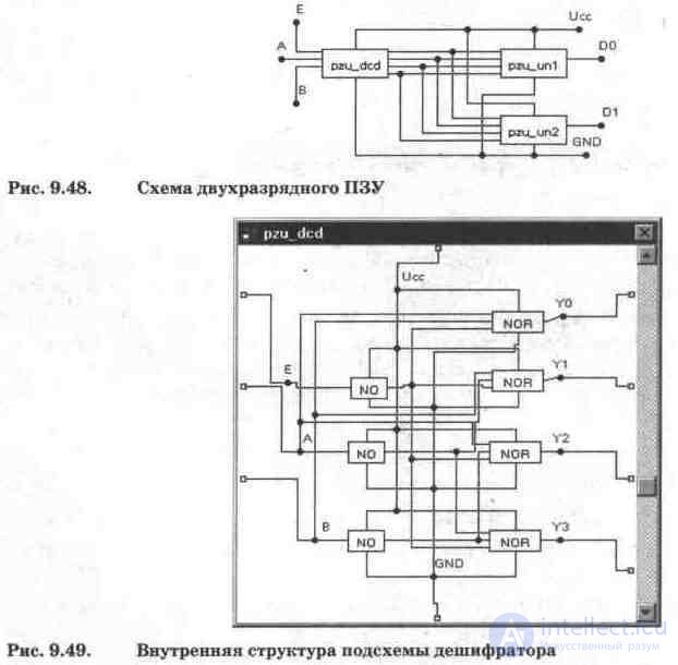
Consider a ROM of the second type, which consists of an nx2n decoder and OR circuits connected to its outputs with fusible jumpers (Fig. 9.48). The ROM contains a 2x4 descrambler in the form of a pzti_dcd subcircuit (A, B are code inputs, E is a permission input, high-level active signal), to the outputs of which you can connect four 4 OR elements with additional devices. In fig. 9.48 shows two such elements made in the form of separate subcircuits pzu_unl and pzu_un2. Although these elements are the same, building them up on the diagram by copying is excluded due to the presence of burnable jumpers - if there are similar subcircuits, burning a jumper in one subcircuit will automatically lead to burning the same jumper in another. Since the program does not allow copying of subcircuits with their renaming, all of them have to be completely executed. In the DO, D1 circuit, the outputs of the lower and first bits.
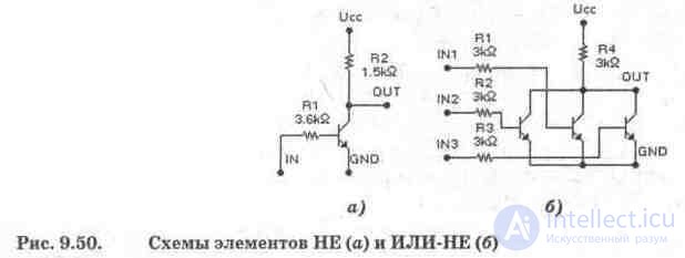
The scheme of the pzu_dcd decoder is shown in Fig. 9.49. The decoder is made on three elements NOT and four elements ZILI-NOT on transistors (Fig. 9.50).
The need to implement decoder elements on transistors is explained by the fact that the mathematical models of digital integrated circuits used in the EWB program do not always allow connecting conventional transistor circuits to them and, in particular, the memory cells used in the ROM in the form of a pzu_uni subcircuit. Its internal structure is similar to the structure of the memory cell used in the K155REZ ROM (Fig. 9.51) [5]. In contrast to the IC K155REZ, in which a multi-emitter transistor is used as an OR element, in Fig. Fig. 9.51 shows the individual transistors T1 ... T4, the emitters of which are connected through the jumpers S1 ... S4 (simulated with 10 mA fuses) to the driver on transistors T5, T6 and the zener diode D. The transistor T5 and the zener diode D are used only in programming mode and in operating mode, they do not affect the operation of the output stage on transistor T6 (cascade with an open collector), since transistor T5 is closed with a low potential at its base (the breakdown voltage of the zener diode D is selected slightly higher than the supply voltage ora T6 supplied to the second subcircuit in DO or point D1 through the load resistor).
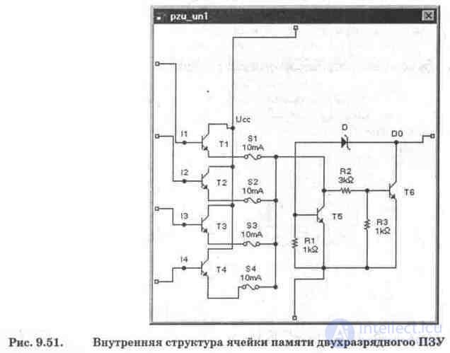
The ROM cell works as follows. In the initial state, the transistors T1 ... T4 and T6 are closed, and when the load is connected to T6, a signal of a logical unit is formed at its DO output (about +5 V). When a given code combination is supplied to the inputs A and B of the decoder, and the input of the resolution E is a logical unit signal, one of the transistors T1 ... T4 opens and a logic zero signal is generated at the DO output. So, for example, at A = B = 1, the transistor T4 opens and the signal of the logical unit from its emitter through the jumper S4 goes to the divider on resistors R2, R3, the transistor T6 opens, and a logic zero signal is generated at its output. Obviously, with any other binary combination, the same thing will happen until the corresponding jumper is destroyed.
The ignition of jumpers is the essence of programming and is carried out separately for each discharge (each cell) as follows:
О binary inputs corresponding to the address of the fired jumper in the programmed bit (in cell pzu_unx, where x is the cell number) are supplied to inputs A and B (see Fig. 9.48);
О A voltage source of 12.5 V is connected to the output of the Dx cell through the load resistor (its resistance for specific ICs is indicated in the documentation, for K155REZ is about 300 Ohms), as a result, the Zener diode breaks and the transistor T5 opens;
О a logic unit signal is applied to the permission input E for a short time, while a sufficient current flows through one of the open transistors T1 ... T2 and T5 to burn the corresponding jumper (the duration of the enable signal at input E in industrial programmers can automatically increase after several unsuccessful attempts to program the same cell);
О The 12.5 V source is turned off, and after opening the corresponding subcircuit, you can make sure that the jumper is really destroyed (in industrial programmers, this process reduces to checking the recording of the programmable cell, and if the result is negative, reprogramming is performed with a longer duration of the enable signal).
The final stage of programming serial ROM chips in an industrial environment is electrical heating, which is most often carried out for 168 hours at elevated temperatures, after which additional control of the recorded information is performed. If an error is detected, re-programming is allowed. If the error repeats again, the chip is rejected.

To simulate the programming process, additional elements must be connected to the programmable circuit. It is advisable to start modeling with a single-bit ROM (Fig. 9.52).
It should be noted that the ROM model under consideration (both in Fig. 9.48 and Fig. 9.52) is rather capricious and modeling is not performed for some combinations of input signals. A sign of the impossibility of modeling is the absence of a window to the left of the power switch (in the upper right corner of the screen) with an indication of the countdown time intervals. After some time, a recommendation may be made to change the simulation error setting (by default, it is 1%). It is advisable to set it as high as possible (10%) in the Circuit menu (Analysis Options command, Tolerance parameter). It is also advisable to vary the resistance of the input resistors and the load resistors of the elements NOT and OR NOT (Fig. 9.50), and also try to change the parameters of the transistors. In an extreme case, you can restrict yourself to the simplest case - do without a decoder and use only one memory cell in Fig. 9.51, connecting additional elements to the output and to one of its inputs, as shown in Fig. 9.52.
ROMs with burnable jumpers are most often used as specialized decoders, for example, for the selection of explosives.
ROMs with ultraviolet erasure are used in microprocessor systems for storing control programs, in particular, for placing the BIOS (Basic Input / Output System - the main input / output system recorded in ROM, hence its full name ROM BIOS) [22]. The BIOS is a set of programs for checking and servicing computer hardware and acts as an intermediary between the operating system (OS) and the hardware. The BIOS receives control when the motherboard is turned on, tests the motherboard itself and the main blocks of the computer - a video adapter, keyboard, disk and input / output controllers, sets up the board's chipset and loads an external OS. When running DOS / Windows З.х / 95/98, the BIOS manages the main devices, while running under OS / 2, Unix, and Windows NT, the BIOS is practically not used, performing only an initial check and configuration.
Usually, only a ROM with a system (Main System) BIOS is installed on the system board, which is responsible for the board itself and the controllers FDD (floppy disks), HDD (hard disks), ports and keyboards; the system BIOS almost always includes System Setup - a system setup program. Video adapters and HDD controllers with ST-506 (MFM) and SCSI interface have their own BIOS in separate ROMs;
other boards can also have them - intelligent disk and port controllers, network cards, etc.
Typically, BIOS for modern motherboards is developed by one of the specialized companies: Award Software, American Megatrends (AMI), less often:
Phoenix Technology, Microid Research; currently the most popular BIOS company Award. Some board manufacturers (such as IBM, Intel, and Acer) are developing the BIOS for them themselves. Sometimes for the same board there are BIOS versions of different manufacturers, in this case it is allowed to copy firmware or replace ROM chips; in general, each BIOS version is tied to a specific model of the board.
Previously, the BIOS was placed in a one-time programmable ROM or ROM with ultraviolet erasure; Now, mainly boards with electrically reprogrammable ROMs (Flash ROMs) are produced, which allow BIOS reprogramming using the board itself. This allows you to correct factory errors in the BIOS, change the factory default settings, program your own screen savers, etc.
The type of ROM chip can usually be identified by the marking: 27xxxx - regular ROM, 28xxxx or 29xxxx - reprogrammable. If there is a transparent window on the case of the 27xxxx chip, this is a ROM with ultraviolet erasure;
if it is not, it is a one-time programmable ROM, which can only be replaced with another.
Video ROM (Video ROM) - a permanent storage device in which video BIOS, screen fonts, service tables, etc. are written. The ROM is not used directly by the video controller, it is accessed only by the central processor; as a result of the execution of the programs recorded in the ROM, the video controller and video memory are accessed. Many modern graphics cards are equipped with electrically reprogrammable ROMs (EEPROM, Flash ROM) that allow the user to overwrite under the control of a special program from the card kit.
ROM is necessary only for the initial launch of the video adapter and work in DOS, Novell Netware and other OSs, which operate primarily in text mode; Windows, OS / 2, and the like, working through their own video drivers, do not use ROMs to control the adapter or use it only when running DOS programs.
When creating a video BIOS, all developers adhere to the recommendations of VESA and VBE. VESA (Video Electronics Standards Association) is an organization that produces various standards in the field of electronic video systems and their software. VBE (VESA BIOS Extension - VESA standard BIOS extension) - additional functions of the video BIOS in relation to the standard video BIOS for VGA, allowing you to ask the adapter for a list of supported video modes and their parameters (resolution, color, addressing methods, sweep, etc.) n.) and change these parameters to match the adapter with a specific monitor. In fact, VBE is a unified standard for the software interface with VESA-compatible cards; when working through the video BIOS, it eliminates the need for a specialized video card driver.
Test questions and tasks
1. What types of ROMs exist and where are they used?
2. What is the BIOS for a computer, video controller, hard disk drive (hard drive) and other peripheral devices?
3. What types of ROMs are used to store BIOS programs?
4. Using the circuit in fig. 9.52, simulate the programming process of ROM with burnable jumpers.
5. Make a ROM diagram based on a two-bit ROM in fig. 9.48 and simulate the programming process of one of its memory cells.

Comments
To leave a comment
Digital devices. Microprocessors and microcontrollers. computer operating principles
Terms: Digital devices. Microprocessors and microcontrollers. computer operating principles