Lecture
Random access memory (RAM) are an integral part of microprocessor systems for various purposes. RAM are divided into two classes: static and dynamic. In static RAM, information is stored on triggers, and in dynamic - on capacitors with a capacity of the order of 0.5 pF. The duration of information storage in static RAM is not limited, while in dynamic it is limited by the capacitor self-discharge time, which requires special means of regeneration and additional time spent on this process.
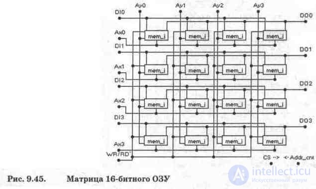
Structurally, any RAM consists of two blocks - a matrix of storage elements and an address decoder. For technological reasons, the matrix most often has a two-coordinate decryption of the address - in rows and columns. In fig. 9.45 shows a matrix of 16-bit static RAM. The matrix consists of 16 mem_i memory cells, the circuit of which is shown in Fig. 9.46. Each memory cell is addressed at inputs X, Y by selecting address lines by the decoders along the lines AxO ... Ax3 and through the columns AuO ... Au3 (see Fig. 9.45) and supplying a logical unit signal along the selected lines. At the same time, a two-input AND element (U1) is triggered in the selected memory cell, preparing information read-write circuits on the input DIO ... DI3 or output DOO ... D03 bit buses. The permissive signal for issuing the address is CS (chip select - chip selection), which is fed to the address counter resolution input (Addr_cnt) or the same input of decoders connected to the counter outputs.
When writing to a memory cell (see Fig. 9.46), 1 or 0 is set on the corresponding bit bus, signal 1 is set at the input WR / RD 'and, after the counter or address decoders are gated, the CS signal triggers elements 2I U1, U2. A positive signal difference from element U2 is fed to the clock input of the D-flip-flop U4, as a result of which it is written 1 or 0 depending on the signal level at its D-input.
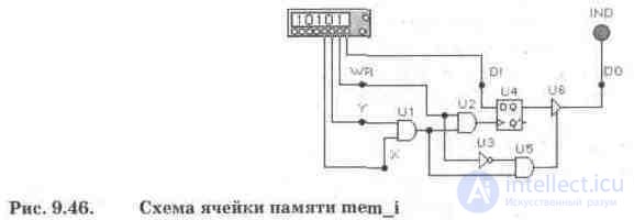
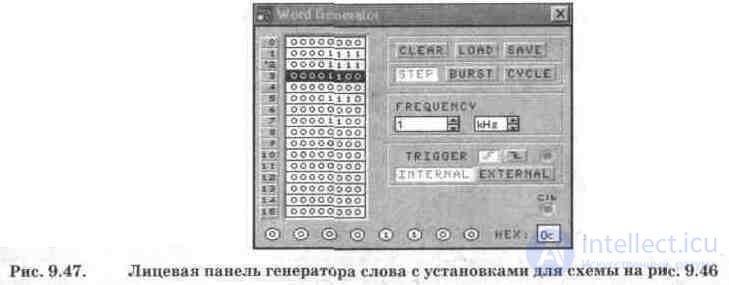
When reading from the memory cell at the input WR / RD ', 0 is set, and the elements U1, U3, U5 are triggered and the ENABLE EXIT of the buffer element U6 receives an enable signal, as a result of which the signal from the Q-output of the D-trigger is transmitted to the discharge bus DOO ... D03. To check the functioning of a memory cell, a word generator is used (Fig. 9.47).
Modern storage devices of static type are characterized by high speed and are used in microprocessor systems only due to the relatively high cost. In such systems, they are used only as the so-called cache memory [22]. Cache (stock) means a high-speed buffer memory between the processor and main memory, which serves to partially compensate for the difference in processor speed and main memory - the most frequently used data is entered into it. When the processor first accesses the memory cell, its contents are copied to the cache in parallel, and in case of repeated access, it can be extracted from it with much greater speed. When writing to memory, information goes to the cache and is simultaneously copied to the memory (Write Through scheme - direct or through writing) or is copied after a while (Write Back scheme - write back). When writing back, also called buffered pass-through recording, information is copied to memory in the first free cycle, and in delayed (Delayed Write) - when there is no free area to put a new value in the cache; at the same time, comparatively rarely used data are pushed into the main RAM. The second scheme is more efficient, but also more complex due to the need to maintain the content of the cache and the main memory.
The cache memory consists of a data area divided into blocks (lines), which are the elementary units of information during the cache operation, and a tag area describing the state of the lines (free, busy, marked for rewriting, etc.). Basically, two cache organization schemes are used: direct mapped, when each memory address can be cached by only one line (in this case, the line number is determined by the least significant bits of the address), and by the ha-connected associative when Each address can be cached in multiple lines. Associative cache is more complex, but allows more flexible data caching; The most common are four-linked caching systems.
Microprocessors 486 and higher also have an internal cache of 8 ... 16 Kbytes. It is also designated as Primary (primary) or LI (Level I - the first level) in contrast to the external (External) located on the board and indicated by Secondary (secondary) or L2. In most processors, the internal cache works according to the direct write scheme, and in 486 (the Intel P24D processor and the latest DX4-100, AMD DX4-120, 5x86) and Pentium it can also work with deferred recording. The latter requires special support from the motherboard, so that when exchanging via DMA (direct access to the memory of I / O devices), it is possible to maintain consistency of data in the memory and the internal cache. Pentium Pro processors also have a built-in second-level cache of 256 or 512 KB.
In microprocessor systems, dynamic RAM with a storage capacitor, which are very diverse, is most often used as RAM. We give data on the most common types of such RAM [22].
In dynamic memory, cells are made on the basis of areas with the accumulation of charges, occupying a much smaller area than triggers, and practically consuming no energy when storing information. When a bit is written to such a cell, an electric charge is formed in it, which remains for several milliseconds; To constantly save the cell charge, it is necessary to regenerate (overwrite) its contents. The cells of dynamic memory chips are also organized in the form of a rectangular matrix; when accessing the microcircuit, its inputs are first supplied with the address of the matrix row followed by the RAS signal (Row Address Strobe); then, after a while, the column address followed by the CAS signal (Column Address Strobe is the column address strobe). Each time a single cell is accessed, all cells of the selected row are regenerated, therefore, to completely regenerate the matrix, it suffices to sort out the addresses of the rows. Dynamic memory cells have a relatively low speed (tens to hundreds of nanoseconds), but a higher specific gravity (of the order of several megabytes per case) and lower power consumption.
Conventional RAMs are often called asynchronous, since the setting of the address and the supply of control signals can be performed at arbitrary points in time, it is only necessary to observe the time relationships between these signals. They include the so-called guard intervals necessary for the establishment of signals. There are also synchronous types of memory that receive an external clock signal, to the pulses of which the moments of address supply and data exchange are rigidly attached; they allow better use of internal pipelining and block access.
FPM DRAM (Fast Page Mode DRAM - dynamic memory with fast page access), is actively used recently. The paged memory differs from conventional dynamic memory in that after selecting the matrix row and holding the signal, the RAS allows multiple setting of the column address gated by the CAS signal, as well as quick regeneration according to the “CAS before RAS” scheme. The first allows you to speed up block transfers when the entire data block or part of it is inside the same row of the matrix, called a page in this system, and the second is to reduce the time spent on memory regeneration.
EDO (Extended Data Out - extended data retention time on the output) are actually ordinary FPM chips, the output of which is set data latch registers. When paging, these microcircuits operate in a simple pipeline mode: they hold the contents of the last selected cell at the data outputs, while the addresses of the next selected cell are already fed to their inputs. This makes it possible to speed up the process of reading sequential data arrays by about 15% compared to FPM. With random addressing, such a memory is no different from ordinary memory.
BEDO (Burst EDO - EDO with block access) is an EDO-based memory that works not in single but in packet read / write cycles. Thanks to internal and external caching of instructions and data, modern processors exchange mainly blocks of words of maximum width with the main memory. With the presence of BEDO memory, there is no need to constantly supply sequential addresses to the inputs of the microcircuits with observance of the necessary time delays; it is enough to gate the transition to the next word with a separate signal.
SDRAM (Synchronous DRAM - synchronous dynamic memory) - memory with synchronous access, faster than regular asynchronous (FPM / EDO / BEDO). In addition to synchronous access, SDRAM uses an internal division of the memory array into two independent banks, which allows combining a sample from one bank with setting the address in another. SDRAM also supports block sharing. The main advantage of SDRAM is the support of synchronous sequential access, where no additional clock cycles are required. With random access, SDRAM runs at almost the same speed as FPM / EDO.
PB SRAM (Pipelined Burst SRAM - static memory with block pipelined access) is a type of synchronous SRAM with internal pipelining, due to which the data exchange rate is approximately doubled.
In addition to the main RAM, a memory display device is also equipped with a display device - a video display system. Such memory is called video memory and is located on the video card.
Video memory is used to store images. The maximum possible resolution of the video card depends on its volume - AxBxC, where A is the number of dots horizontally, B is the vertical, C is the number of possible colors for each point. For example, for a resolution of 640x480x16, it is enough to have 256 KB of video memory, for 800x600x256 - 512 KB, for 1024x768x65536 (another designation is 1024x768x64k) - 2 MB, etc. Since an integer number of digits is allocated for storing flowers, the number of colors is always an integer power of 2 (16 colors - 4 digits, 256 - 8 digits, 64k - 16, etc.).
Video adapters use the following types of video memory.
FPM DRAM (Fast Page Mode Dynamic RAM) is the main type of video memory that is identical to that used in motherboards. It was actively used until 1996. The most common FPM DRAM chips are four-bit DIP and SOJ, as well as sixteen-bit SOJ.
VRAM (Video RAM - video RAM) - the so-called dual-port DRAM with support for simultaneous access from the video processor and the central processor of the computer. Allows you to combine in time the output of the image on the screen and its processing in the video memory, which reduces delays and increases the speed of work.
EDO DRAM (Extended Data Out DRAM - dynamic RAM with extended data retention time on the output) - memory with pipelining elements, which allows to somewhat speed up the exchange of data blocks with video memory.
SGRAM (Synchronous Graphics RAM) is a DRAM option with synchronous access, when all control signals are changed simultaneously with the system clock, which reduces time delays.
WRAM (Window RAM) - EDO VRAM, in which the window through which the video controller accesses is made smaller than the window for the central processor.
MDRAM (Multibank DRAM - Multibank RAM) - a variant of DRAM, organized in the form of many independent banks of 32 Kbytes each, operating in the pipelined mode.
An increase in the speed of the video processor's access to video memory, in addition to increasing the adapter's throughput, can increase the maximum frequency of image regeneration, which reduces operator eye fatigue.
Memory microcircuits have four main characteristics - type, volume, structure and access time. Type denotes static or dynamic memory, volume indicates the total memory capacity, and the structure indicates the number of memory cells and the capacity of each cell. For example, 28/32-pin SRAM DIP chips have an 8-bit structure (8kx8, 16kx8, 32kx8, 64kx8, 128kx8), a 256KB cache consists of eight 32kx8 chips or four 64kx8 chips (we are talking about data area, additional chips for storage of attributes may have a different structure). Two 128kx8 microcircuits can no longer be delivered, since a 32-bit data bus is needed, which can only be provided by four microcircuits. Common SRAM PBs in 100-pin PQFP packages have a 32-bit 32kx32 or 64kx32 structure and are used in two or four in Pentium boards.
30-pin SIMMs have an 8-bit structure and are used with two processors 286, 386SX and 486SLC, and four with 386DX, 486DLC and regular 486DX. 72-pin SIMMs have a 32-bit structure and can be used with 486DX one at a time, and with Pentium and Pentium Pro, two at a time. 168-pin DIMMs have 64-bit structures and are used by Pentium and Pentium Pro one at a time. Installing memory modules or cache chips in an amount greater than the minimum for a given system (motherboard) board allows you to speed up work with them using the Interleave principle.
Access time characterizes the speed of the chip and is usually indicated in nanoseconds after the dash at the end of the name. On slower circuits, only the first digits can be indicated (-7 instead of -70, -15 instead of -150), on faster static “-15” or “-20” indicates the real time of access to the cell. Frequently, the minimum of all possible access times is indicated on microcircuits, for example, the marking is 50 EDO DRAM instead of 70, or 45 instead of 60, although such a cycle is achievable only in block mode, and in single mode the microcircuit still has an access time of 70 or 60 ns. A similar situation occurs in the marking of the SR SR: 6 instead of 12, and 7 instead of 15. SDRAM chips are usually marked with access time in block mode (10 or 12 ns).
Memory ICs are implemented in the following types of cases.
DIP (Dual In line Package - a housing with two rows of pins) - classic microcircuits used in IBM PC / XT and early PC / AT main memory blocks are now used in cache blocks.
SIP (Single In line Package - housing with one row of pins) - a chip with one row of pins, mounted vertically.
SIPP (Single In line Pinned Package - module with one row of needle pins) - a memory module that is inserted into a panel like DIP / SIP chips; used in early IBM PC / AT.
SIMM (Single In line Memory Module - a memory module with one row of contacts) - a memory module inserted into the clamping socket; It is used in all modern motherboards, as well as in many adapters, printers and other devices. SIMM has contacts on both sides of the module, but they are all interconnected, forming as if one row of contacts. Most SIM cards currently use FPM / EDO / BEDO chips.
DIMM (Dual In line Memory Module - a memory module with two rows of contacts) is a memory module similar to SIMM, but with separate contacts (usually 2x84), which increases the capacity or number of memory banks in the module. It is mainly used in Apple computers and new motherboards P5 and P6. EDO / BEDO / SDRAM chips are installed on the DIMM.
CELP (Card Egde Low Profile - a low card with a knife connector on the edge) is an external cache module assembled on SRAM (asynchronous) or PB SRAM (synchronous) chips. In appearance it is similar to a 72-pin SIMM, it has a capacity of 256 or 512 KB. Another name is COAST (Cache On A STick - literally "stick cache").
Dynamic memory modules, in addition to the main memory cells, can have additional cells for storing parity bits for data bytes; such SIMMs are sometimes called 9- and 36-bit modules (one parity bit per data byte). Parity bits are used to control the correct reading of data from the module, allowing to detect part of the errors (see section 9.7). Modules with parity bits only make sense where very high reliability is needed. Well-tested modules with no parity bits are also suitable for common applications, but provided that the system board supports these types of modules.
The easiest way is to determine the type of module by marking and the number of memory chips on it: for example, if on a 30-pin SIMM there are two chips of the same type and another one of the other, then the first two are primary (each - four bits), and the third is intended for storage parity bits (it is single-bit).
In a 72-pin SIMM with twelve chips, eight of them store data, and four store parity. Modules with the number of chips 2, 4 or 8 do not have memory for storing parity bits.
Sometimes a so-called parity simulator is placed on the modules — an adder chip that always gives the correct parity bit when reading a cell. This is mainly intended for installing such modules in boards where the parity check is not disabled.
72-pin SIMMs have four special PD (Presence Detect) lines, on which up to 16 signal combinations can be set using jumpers.PD lines are used in some motherboards to determine the presence of memory modules in the connectors and their parameters (volume and speed). Most third-party universal boards, like SIMMs they produce, do not use PD lines.
In DIMMs, in accordance with the JEDEC specification, PD technology is implemented using a rewritable serial access memory (Serial EEPROM) and is called Serial Presence Detect (SPD). The ROM is an 8-pin chip located in the corner of the DIMM board, and its contents describe the configuration and parameters of the module. Motherboards with 440LX / BX Chipset can use SPD to configure the memory management system. Some motherboards can do without SPD by defining the configuration of modules in the usual way.
Test questions and tasks
1. What types of memory exist?
2. Simulate the static memory cell in Figure 2. 9.46. The modeling task is to select binary combinations for signals at the input of the cell and register the result at the output of the cell using the IND indicator.
3. Based on the circuit in Fig. 9.45 develop a four-bit RAM circuit using a word generator. Moreover, in the diagram in Fig. 9.45 use only 4 lower addresses (two in rows and two in columns) and, accordingly, only two data buses (two input and two output). Connect indicators to the output buses.
4. Where do modern computers use static type memory?
5. What is the difference between dynamic memory and static?
6. What types of dynamic memory are used in modern computers?
7. What is video memory and how is it related to the characteristics of the information displayed on the display?
8. What types of memory are used as video memory?
9. What is the design of the memory chips?

Comments
To leave a comment
Digital devices. Microprocessors and microcontrollers. computer operating principles
Terms: Digital devices. Microprocessors and microcontrollers. computer operating principles