Lecture
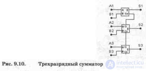
Arithmetic adders are an integral part of the so-called arithmetic logic devices (ALU) of microprocessors (MP). They are also used to form the physical address of memory cells in MP with segmented memory organization. In the EWB program, arithmetic adders are represented in the Comb'I library by two basic devices, shown in Fig. 9.9: half adder and full adder. They have the following assignment of conclusions: A, B - inputs of terms,? - the result of the summation. Co is the transfer output, Ci is the transfer input. A multi-bit adder is created on the basis of one half-adder and full adders. As an example in fig. 9.10 shows the structure of a three-digit adder [20]. The first and second terms are applied to the inputs Al, A2, A3 and Bl, B2, and ВЗ, respectively, and the summation result is taken from the outputs SI, S2, S3.

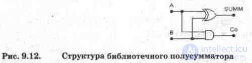
To study the internal structure and logic of the operation of adders, the logical converter is the best suited. After connecting the half-adder to the converter according to fig. 9.11, and sequentially press the buttons  "pack .. as a result, we obtain a truth table and a Boolean expression. Comparing the data obtained with the results of studying the basic logic elements in the previous section, we conclude that when connecting the output (half-adder to the OUT terminal of the converter (as shown in Fig. 9.11, a) it performs the functions of an exclusive OR element.Connecting the OUT terminal of the converter to the output from the half-adder and doing the same, we conclude that in such a turn-on, the half-adder performs the functions of element I. Therefore, it is equivalent to The half-adder circuitry has the form shown in Fig. 9.12.
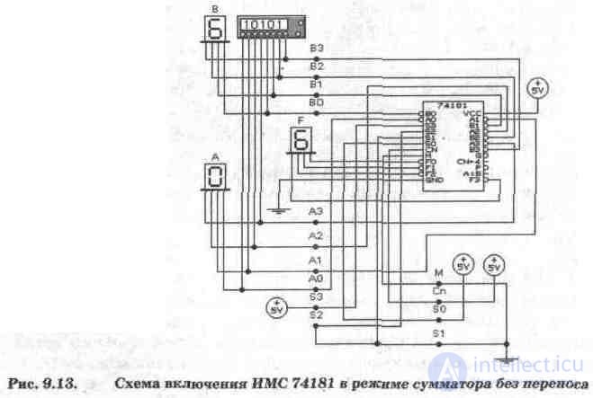
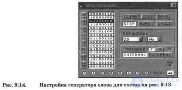
"pack The EWB 4.1 program directory contains a four-bit ALU switching circuit (alul81.ca4 file) based on the serial chip 74181 (domestic analogue of K155IPZ [5, 7]). In a slightly revised form, it is shown in Fig. 9.13. IMS 74181 provides 32 operating modes ALU, depending on the state of the control signals at the inputs M, SO ... S3, and also allows for a bit increase (CN input and CN output <4 for transfers). The IC switching circuit shown in Fig. 9.13 corresponds to the adder mode without transfer. operands A and B at the input are set with help Using a generator and words in a hexadecimal code, alphanumeric indicators of the same name are displayed.On the outputs FO ... F3, the summation result is displayed by the indicator F. By changing the state of the signals at the control inputs, you can simulate most of the ALU functions used in microprocessors (see Sec. 5.14). The operating modes of the word generator in the circuit in Fig. 9.13 and its code set are shown in Fig. 9.14.

Test questions and tasks
1. What is the difference between a half adder and a full adder?
2. Find out the internal structure of the full adder using the scheme of its connection to the logic converter in Fig. 9.11, b and taking into account the methodology for solving a similar problem for a half-adder.
3. Using the experience with the circuit in Fig. 9.13, connect to the inputs of the three-digit adder in fig. 9.10 a word generator, and to the outputs - an alphanumeric indicator with a decoder and check that it functions correctly.
4. Check the operation of the IMS 74181 in the adder mode with the transfer (to the input Cn, give a logic zero signal)

Comments
To leave a comment
Digital devices. Microprocessors and microcontrollers. computer operating principles
Terms: Digital devices. Microprocessors and microcontrollers. computer operating principles