there is a huge pile of applications when the use of the FPGA is not only justified, but also leads to a significant simplification of the system and improvement of its parameters. I’ll just make a reservation: in this and, possibly, subsequent articles, I consider FPGAs only from Xilinx, not because they paid me, and not even because they are the best, just historically, that I work almost exclusively with them.
So let's start with a bit of theory.
FPGAs are divided into two main groups: CPLD (Complex Programmed Logic Device) and FPGA (Field Programmed Gate Array).
CPLD is usually an economy class FPGA, i.e. have a low price and a rather meager amount of resources, this is especially noticeable on triggers.
FPGAs are usually more expensive, contain more resources (simple logic - triggers ...) and, most importantly, lately, additional "complex" blocks, such as multipliers, block memory, interface supplies (Ethernet, PCI-express ... ) and even PowerPC processor cores. Separately, we can mention a series of Zinq from Xilinx - there generally stuffed ARM cores. The main difference between FPGA and CPLD is the need to load the configuration at power up and, accordingly, the external ROM with the configuration. Even the SPARTAN-3AN family has onboard a built-in ROM-shku, from which it is loaded.
Now the most important thing: how does the FPGA differ from the controller and when to use them. Everything is pretty simple here: FPGA (take those without frills) is, in fact, a bag of logic on a single chip, which can be arbitrarily combined: those same triggers, AND, OR, and similar primitives, such as, for example, in the K155 series or 74ns. The controller is a ready-made processor (albeit with a scant amount of commands), internal memory, data and command buses, peripherals, etc. Generally speaking, a small controller can be made from a large FPGA, but this idea, at least, is a silly one. So, the controller is sharpened for the execution of long chains of commands, their cyclic repetition, switching from one chain to another, etc., and the FPGA is sharpened for performing simple logical operations and, importantly, a large number at once (and even at different clock frequencies) .

FPGA Xilinx XC95288XL in the TQ144 package  Description of the chip Xilinx XC95288XL (pdf datasheet 237 KB) |
Let's move from theory to practice. For a start, we have enough chips CPLD. There are few resources, but for mastering it. I'll take the XC95288XL in the TQ144 package (again, it just turned out to be available), I generally recommend taking something fresher, for example, from the CoolRunner 2 series. To get the finished product (even if it is minimally blinking by the LED), we need to: solder the hardware (here I hope there will be no problems, and I will mention the nuances), "write" the firmware (in our case, rather, draw) and sew the firmware into the chip. In general, we need software, generating firmware, and a programmer. The software (Xilinx ISE Webpack) is downloaded from the official site (although it will be asked to register), the Webpack license is free. The programmer can be made according to the scheme in Figure 1 (for LPT-port) or purchase factory USB-shny (in Chinese online stores I met at a price of about $ 50, but did not buy it myself). In details.
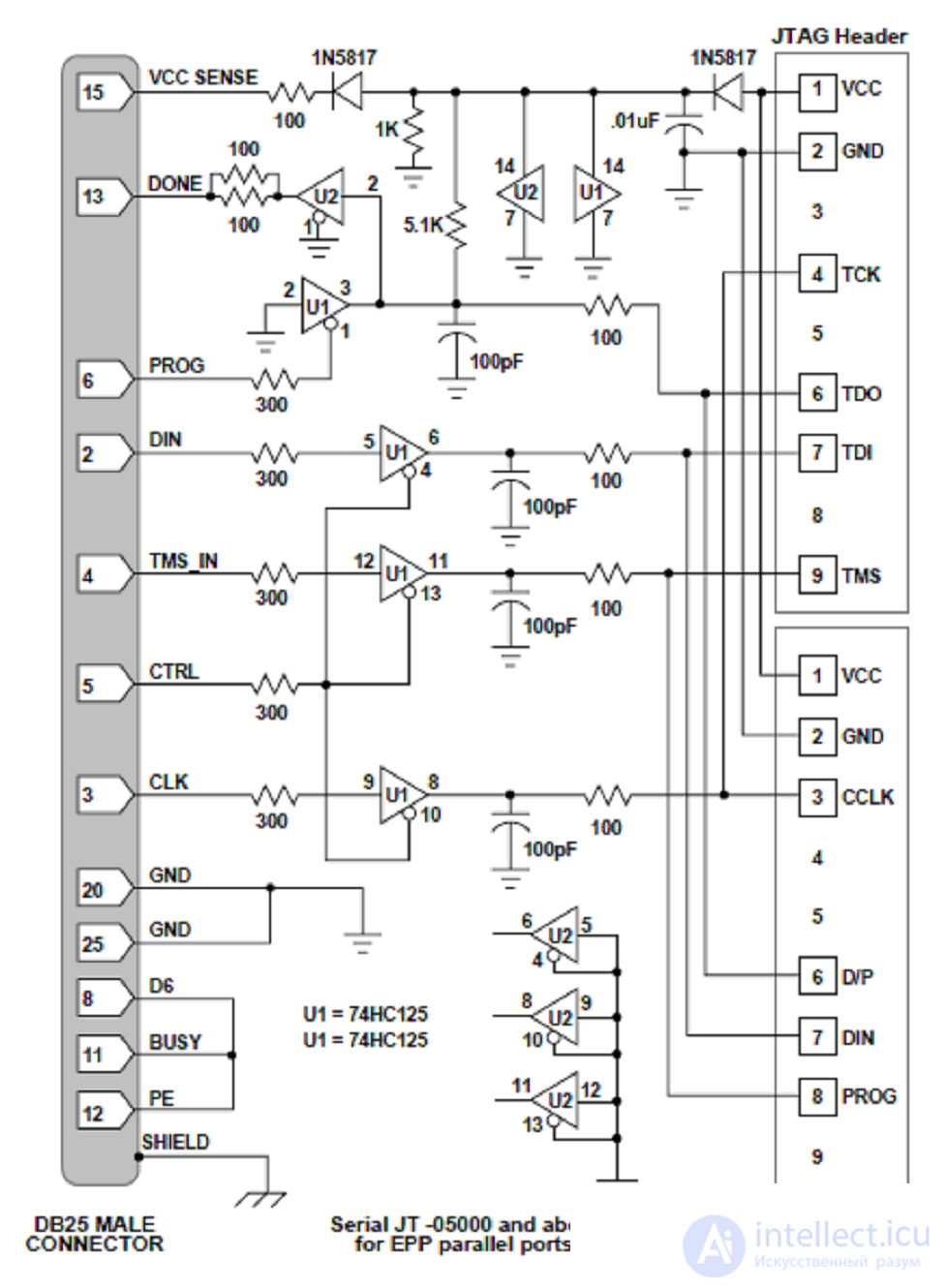
Fig. one
(image is clickable to enlarge, will open in a new window) After we soldered the FPGA to the breadboard, we soldered or bought the programmer, downloaded and installed the ISE Webpack package (I have version 13.2), run Project Navigator and create a new project. To create a project, select File -> New Project, specify the name of the project and where to save it, also indicate the type of source code TOP-LEVEL (Fig. 2). The fact is that for the FPGA it is not necessary to draw a scheme of triggers and their connections, for example, you can write in high-level languages (VHDL, Verilog) and it is not necessary to use one thing within one project. We still use only Schematic at all levels.
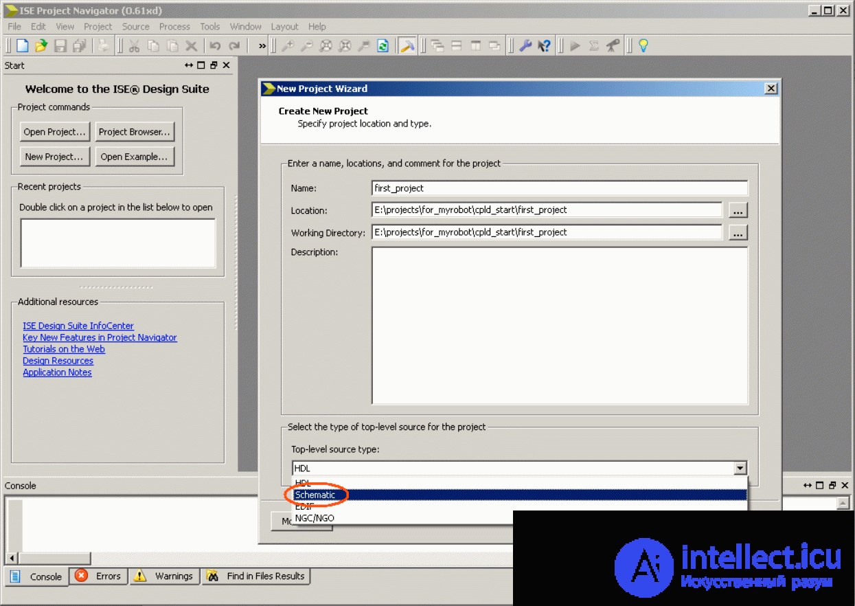
Fig. 2
(image is clickable to enlarge, will open in a new window) In the next window (fig. 3) we select our microcircuit (at first we do not touch the rest); in the window that appears after clicking on the "Next" button, we admire the parameters of the created project, click "Finish" - and the project is complete: the project has been created.
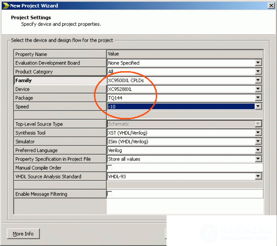
Fig. 3 Now we actually need to draw a scheme: right-click on the window with the project and new sourсe (Fig. 4.), name this source name (this is the name of our scheme, there may be many of them in the project), again select Schematic, click "Next ", we admire the parameters of the newly created file, click" Finish "and get a clean scheme.
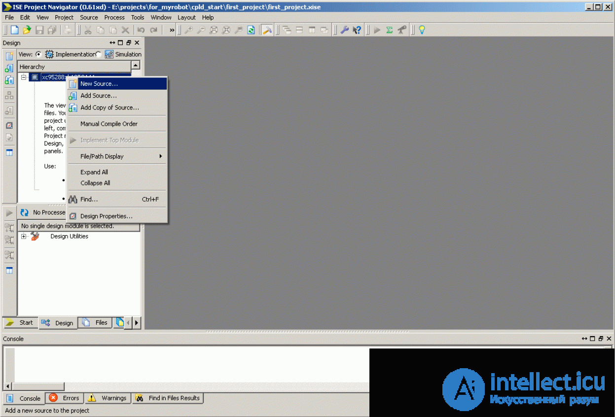
Fig. four
(image is clickable to enlarge, will open in a new window) The most interesting begins: on the panel on the left (not from the very edge), press the "add symbol" button (Fig. 5).
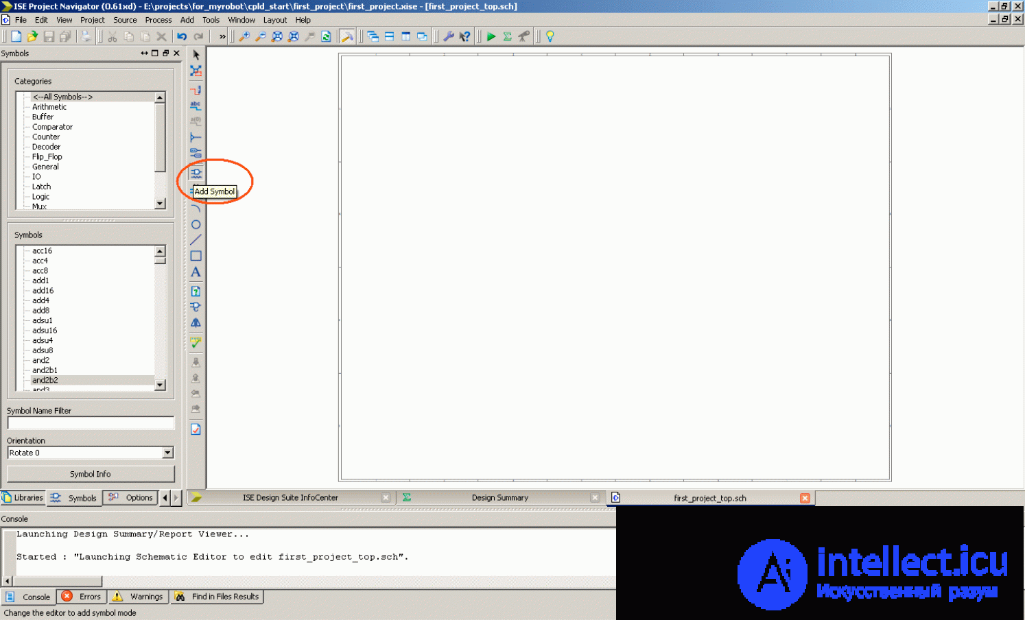
Fig. five
(image is clickable to enlarge, will open in a new window) And we get to the left of the list of characters of the current library. How to add, create, edit libraries, we will understand later (as needed). Now it is important for us to choose the desired symbol. So in the upper window we see a certain classifier - a filter that is not necessary to use (well, why scroll through all sorts of triggers and logic elements when we need a counter).
For example, consider the following task: you need to accurately determine the time delay between the leading edges of 2 pulses appearing on different wires, and merge this value into the controller via the SPI interface. Any similarity of the problem with the topic "Increasing the operating frequency of the MK" on one of the robotic forums is intentional. So, at the device input there are 2 wires for pulses and 3 wires for the SPI controller. Add another clock input (we do not know at what frequency, we can only assume that at least 70 MHz). We start to draw the firmware: we need trigger-latches that will "catch" the pulses, the time counter, the shift register (we don’t need to create them, they are library). I will not describe what triggers and counters are, hopefully the readers are “in the subject line” and there will be no problems, otherwise I will have to write a few more articles. Received just such a scheme (Fig. 6), as you can see, it is not necessary to pull the wire from the output of the symbol to the input, just call the circuit. To designate external inputs and outputs, use the button "Add I / O Marker".
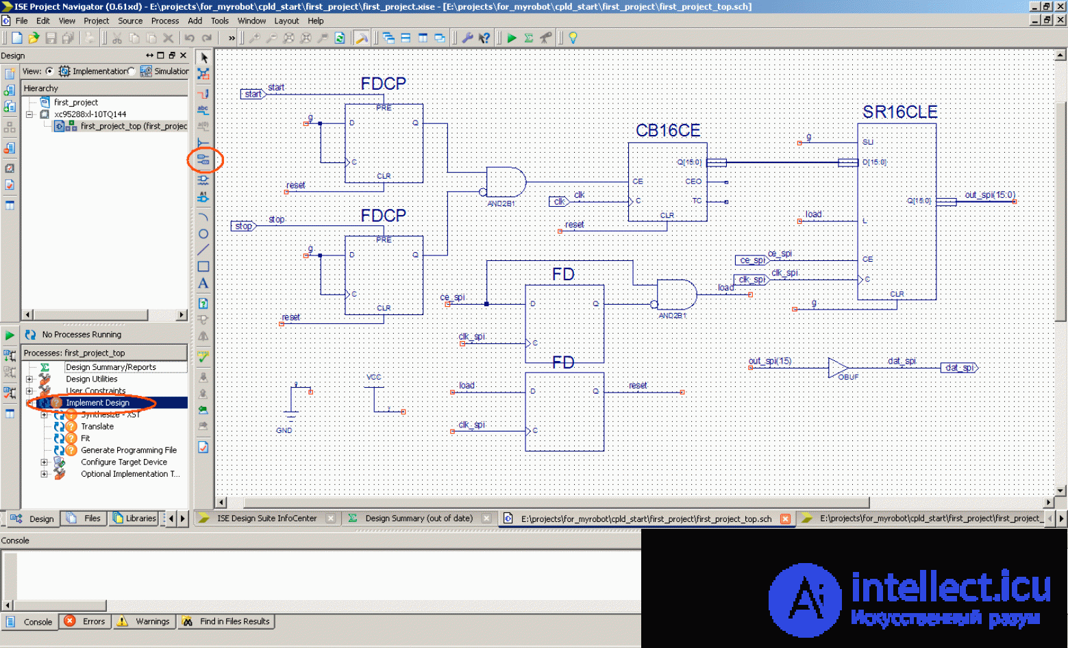
Fig. 6
(image is clickable to enlarge, will open in a new window) When the scheme is ready, go to the Design tab, and add to Implement Design — all processes begin (for a start, it doesn’t matter which ones - the main thing is that all together is the process of distilling the source code into the firmware). When everything works out, we look at the errors with warnings: everything that is important, we correct, we leave the rest. For example, we do not need the CEO and TC outputs of the counter and the remaining 15 bits of the parallel output of the shift register are also not needed, and swears at us. If we swear at the eruptions that we want it, then we want something wrong. If we (and the synthesizer) are satisfied with everything, we admire further reports: how many resources are spent, which clock frequencies are available ... If everything is fine again, then it's time to simulate the circuit and make sure that it actually works according to the task. I propose to carry out a simulation after checking the timings, because sometimes to get the desired clock frequency you have to shake up the whole scheme, which, of course, can affect the result ...
So, the simulation: on the Design tab (in the left panel) we select the simulation (Fig. 7).
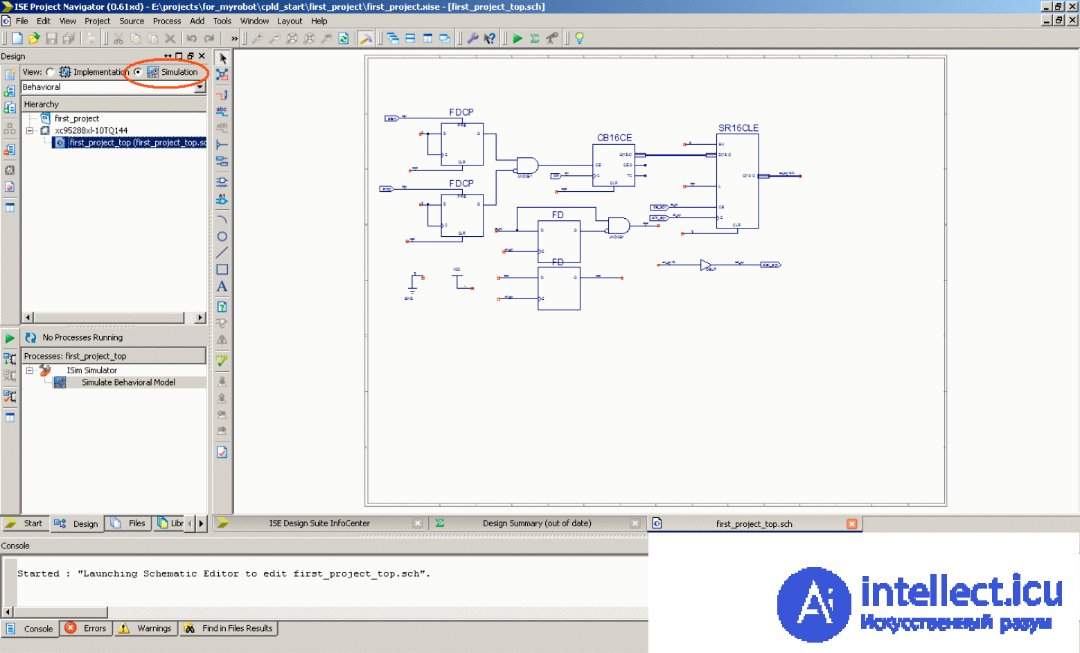
Fig. 7
(image is clickable to enlarge, will open in a new window) Below, in the processes, instead of the processes of synthesis and layout, a Simulate Behavioral Model process has appeared, we are duplicating it — a simulator is launched in which we see our signals (not only input-output, but also intermediate) (Fig. 8).
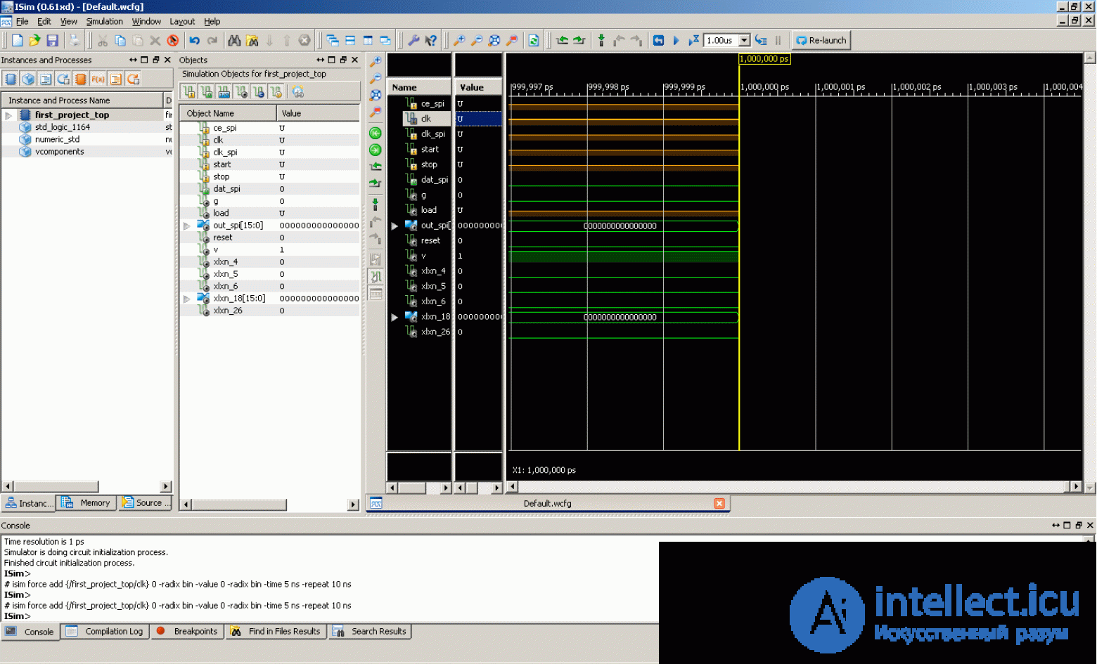
Fig. eight
(image is clickable to enlarge, will open in a new window) Hover the mouse cursor over the buttons, read the comments on the buttons. We set the time of the simulation step (Fig. 9) and the initial values of the input signals, immediately adjust the clock signals (we will not simulate every 5 ns and switch the clock).
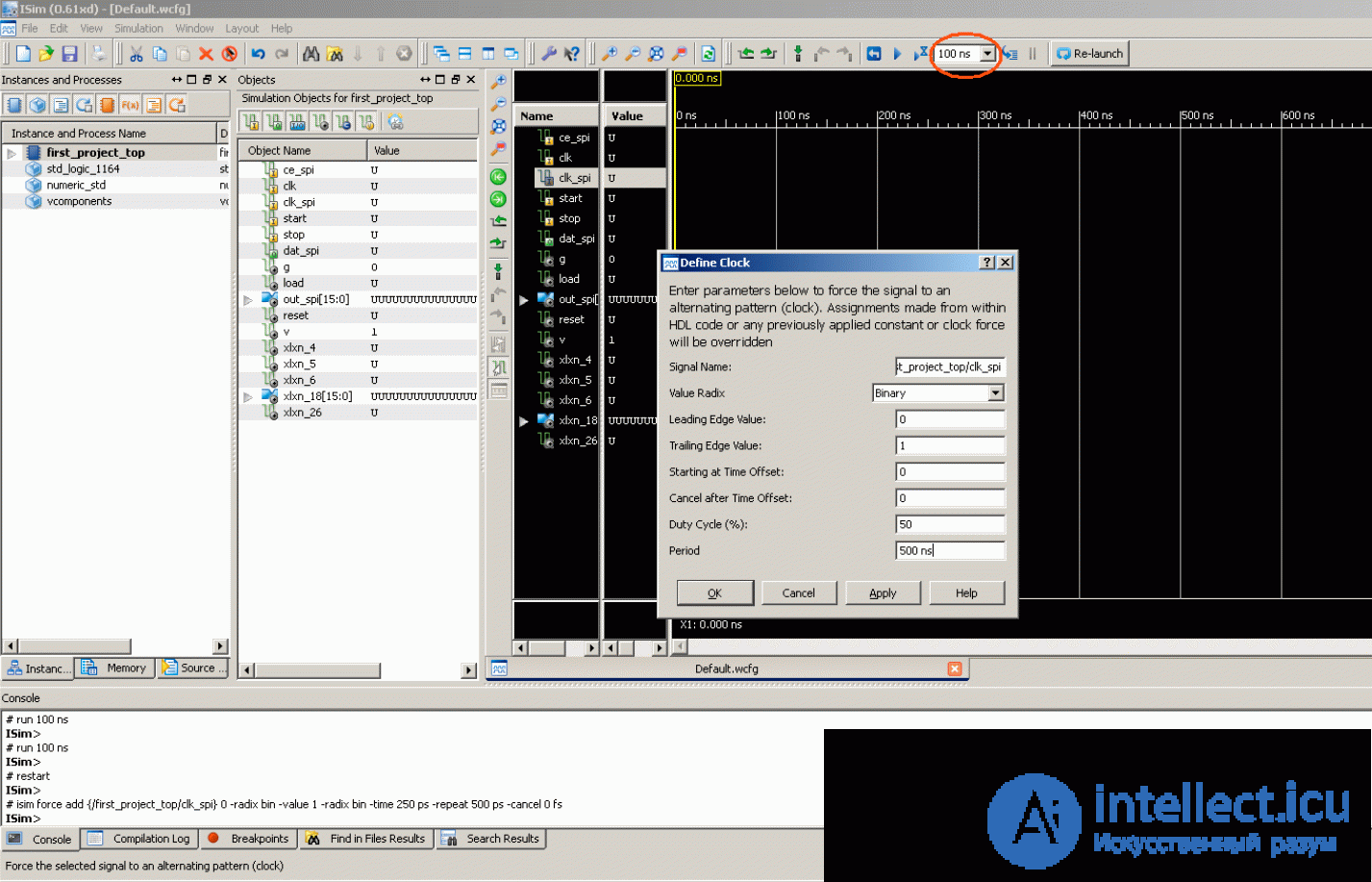
Fig. 9
(image is clickable to enlarge, will open in a new window) Walking in time by manipulating the inputs and (if necessary) with the simulation step, we obtain a timing diagram (Fig. 10).
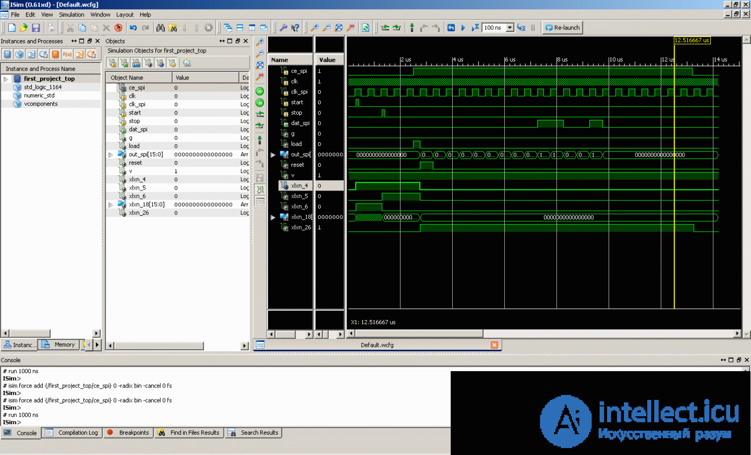
Fig. ten
(image is clickable to enlarge, will open in a new window) Make sure that everything works as planned (or debug the circuit further), and proceed to the next step - the distribution of the outputs and inputs on the legs of the chip. To do this, add another source file (Fig. 11), namely Implementation Constraints File.
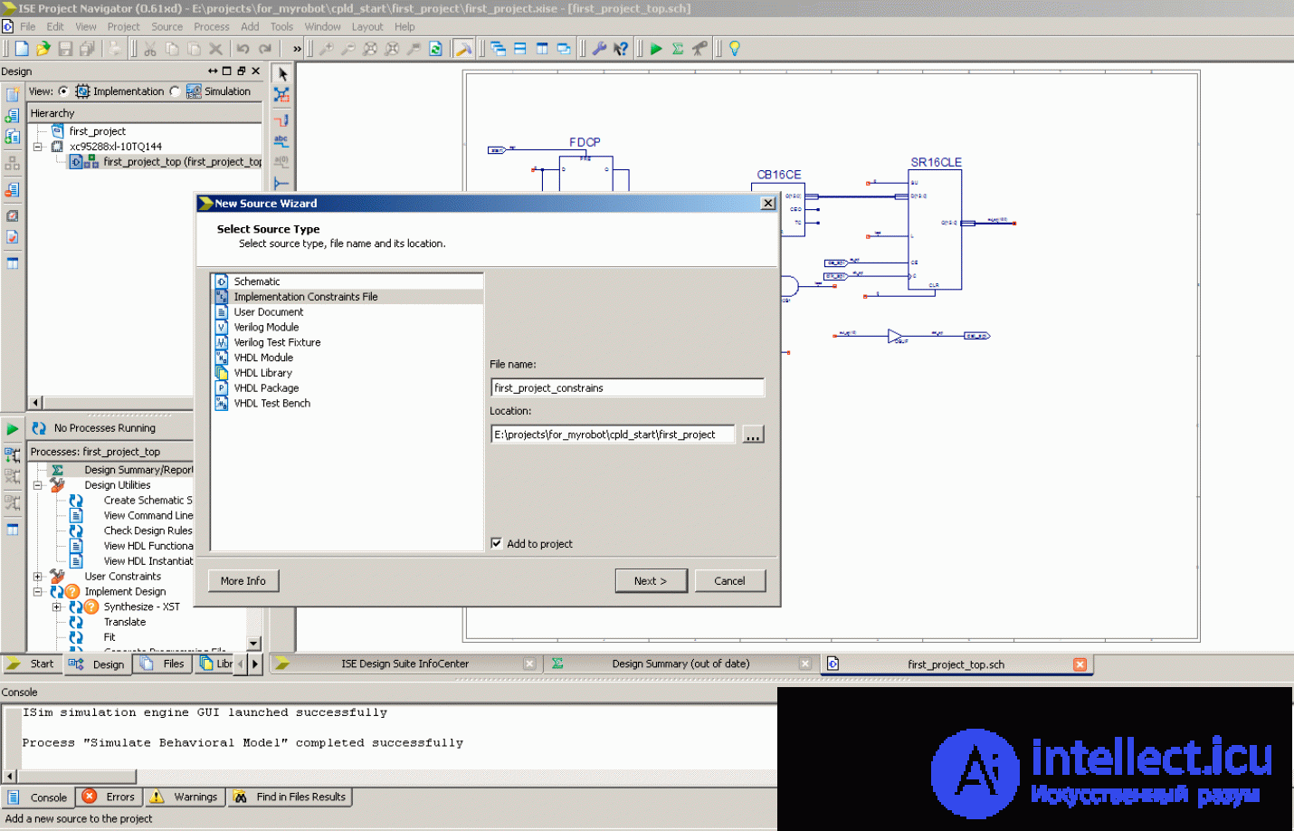
Fig. eleven
(image is clickable to enlarge, will open in a new window) We register the "pinout of the microcircuit" (Fig. 12), here we also prescribe the requirements for clock frequencies. And here we come to the nuance associated with the clock signals. The fact is that the clocking signals must come to the so-called global lines - the lines that pass through the entire microcircuit, the other lines are local in nature and go from block to block through switching logic. The XC95288XL chip in the TQ144 package has 3 such lines, and they are connected to legs 30, 32, 38. The rest of the signals can be connected to any I / O (I / O) legs.
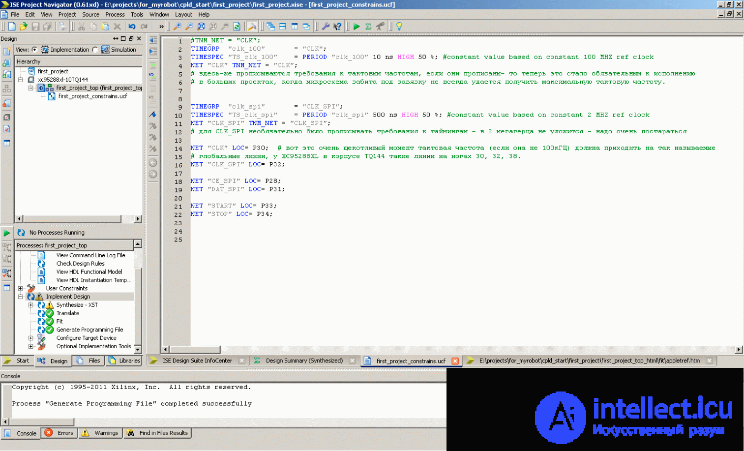
Fig. 12
(image is clickable to enlarge, will open in a new window) Once again we’ve doubled the Implement Design, wait, read the comments on the subject of varning with errores and go to the reports on pinout (Fig. 13) and timing (Fig. 14); we are convinced that everything suits us, and we are lucky in the form of the% project_name% .jed file.
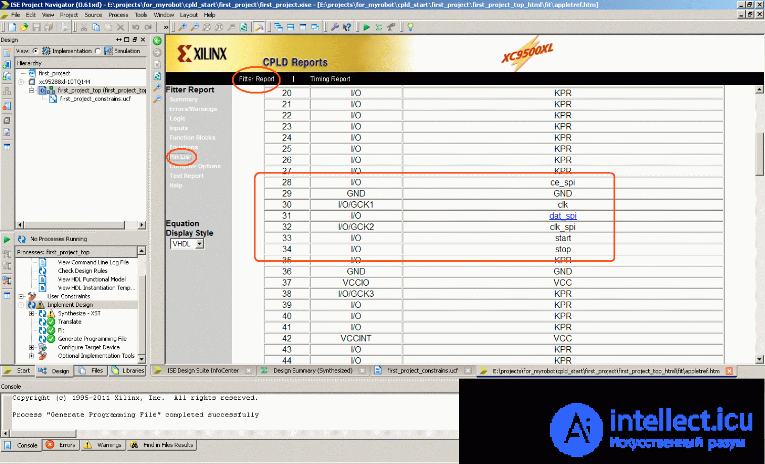
Fig. 13
(image is clickable to enlarge, will open in a new window) 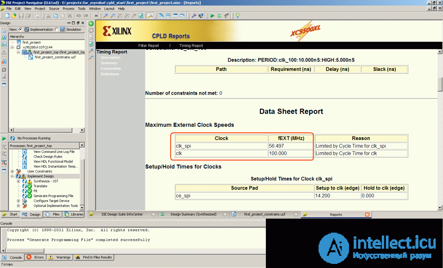
Fig. 14
(image is clickable to enlarge, will open in a new window) The firmware file is ready. Let's say the device too. We connect to the computer JTAG cable and publish on Configure Target Device. The firmware utility (Impact.exe) will start; in fact, when manufacturing several devices for a series firmware, you can limit yourself to running only one of them. We create a new project (this is a project for a firmware program), allow it to automatically find the programmer and the connected chip, display the firmware file and click Program. We are waiting for several tens of seconds, we see the inscription that everything is fine - the device is ready.

Comments
To leave a comment
Digital devices. Microprocessors and microcontrollers. computer operating principles
Terms: Digital devices. Microprocessors and microcontrollers. computer operating principles