Lecture
Mobile stations - MS (Mobile Station) - (mobile phones, cellular radiotelephones, etc.) within each class of the model in a certain standard of cellular mobile communication differ not only in the number of services, but also in the parameters of receiving and transmitting paths, the design, appearance, control unit, etc.
There are a large number and variety of mobile stations on the world market, but all of them have the following typical blocks (Fig. 4.1):
- the control unit, which includes the display and keyboard (sometimes they include a microphone and a telephone);
.
- transceiver unit;
- Antenna unit with switch channels and ranges;
- a logic unit (MS think tank) includes a DSP (Digital Signal Processor) digital processor, sometimes called a CPU (Central Processing Unit), with its DSP Memory, often including equalizer, channel and speech codecs , ADC, DAC, etc .;
- User Identification Module SIM (Subscriber Identity Module)
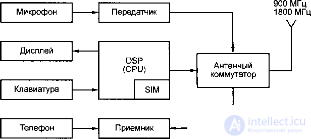
Fig. 4.1. Typical mobile station blocks
4.1. Structural diagram of a mobile station.
The block diagram of a digital mobile station, in this case a digital mobile radiotelephone operating in the GSM standard, is presented in Fig. 4.2. As noted above (Fig. 4.1), all four main blocks (and SIM-card) in Fig. 4.2 deployed in more detail on the main cascades.

Fig. 4.2. Block diagram of a digital radio telephone (MS) of GSM 900 standard
Consider the basic units of a mobile station MS GSM standard.
Antenna unit
Antenna unit includes:
- the antenna itself (in the simplest case, a quarter-wave vibrator (pin), having a length of / - X / 4 = 33.7 / 4 = 8.425 cm, while the antenna performs the functions of a transmitting and receiving antenna (it should be noted that the antenna is often performed as a helical shortened antenna, on the basic parameters similar to a standard half-wave antenna);
- Antenna switch - electronic switch, controlled from the CPU and connecting the antenna input either to the transmitter output or to the receiver input.
In GSM systems, the transmitter and receiver do not work simultaneously and the transmission mode is carried out only for 1/8 of the frame duration. This significantly reduces battery power consumption and increases the operation time both in transfer mode (conversation) and reception mode (standby). In addition, this leads to lower requirements for the high-pass filter of the receiver.
Transmitter Transmitter Unit
Consider the basic blocks of the transmitter (send), their purpose and function.
- Speech signal converted by a microphone (MC) into an electric analog signal and amplified by a low frequency amplifier (ULF) is fed to an analog-to-digital converter (ADC — ADC — Analog-to-Digital Converter), at the output of which the voice signal is converted into digital form and then the speech signal is transmitted digitally.
- A speech coder encodes a speech signal, that is, converts a signal (having a digital form) according to certain laws in order to reduce its redundancy, that is, to reduce the amount of information transmitted over the communication channel.
- The channel coder adds to the digital signal received from the output of the speech coder additional (redundant) information designed to protect against errors during transmission of the signal over the communication line; for the same purpose, the information is subject to a certain repackaging (interleaving); In addition, the channel encoder incorporates control information from the CPU into the transmitted signal.
- I / Q generator is designed to generate a modulating signal from a generated digital signal with direct control from the CPU.
- Phase modulator implements Gaussian manipulation with a minimum frequency shift (GMSK - Gaussian Minimum Shift Keying), that is, realizes the transfer of a digital signal in the region of the radio frequency channel. In the GSM standard with GMSK modulation, the BT product, which determines the cut-off frequency of the pre-modulation Gaussian filter, is VT = 0.3 (where B is the frequency spectrum band, Tj is the message bit duration). This value of the VTL product is achieved by complex hardware implementation to increase the required SI ratio (signal / interference) and reduce the influence of radio wave propagation conditions and equipment imperfection. With GMSK, high efficiency of the power amplifier and acceptable noise immunity are ensured: the probability of error Pe = 10_3 at C / N = 30 dB (C IN - signal-to-noise).
- The mixer (SMP) is designed to transfer the signal at the output of the phase modulator with a frequency / FM to the frequency range 890 ... 915 MHz under the influence of a signal from the frequency synthesizer (ftr) controlled from the CPU.
- A concentrated selection filter (FSS) (usually performed on a silicon filter) is tuned to one of the selected carrier frequency by the CPU and implements filtering of higher harmonics to reduce inter-channel effects.
- The power amplifier (PA) not only amplifies the high-frequency signal from the output of the FSS, but also under the action of commands from the CPU changes the gain (that is, the non-linear gain mode is used), thereby depending on the distance between the mobile MS and the base BTS stations, the output power of the transmitter The MS is automatically regulated: the closer the MS is to the BTS, the lower the MS transmitter power, the less power emitted by the MS antenna.
- The high-frequency signal from the output of the power amplifier through the filter of the concentrated selection (FSS) enters the antenna switch (AK) and in the case of transmitting the speech signal, the CPU switches the AK to the transfer mode.
It should be noted that the path: phase modulator - mixer - FSS - UM - FSS - is often called the GMSK modem (since this path is currently implemented as a single-chip VLSI) and it is used in several European standards.
Thus, the analog part of the transmitter performs the usual functions of transferring information from a coded digital signal to the carrier area of the selected frequency transmission channel, and the digital part, with the active participation of the CPU, processes and transfers information (speech, etc.) in digital form with the addition of information streams. management, protection, addresses, etc.
Consider the main stages of the receiver, their purpose and function.
- The high-frequency signal in the range of 935 ... 960 MHz is received by the antenna and through the antenna switch (turned on by the CPU in receive mode) enters the high-pass filter (usually the surface acoustic wave filter (FPAV) - ceramic filter), is amplified in a high-frequency low-noise amplifier (LNA) .
- The first mixer CM1 allows the signal to be shifted to a lower frequency region, while the second input of the CM1 signal is sent from the frequency synthesizer (controlled from the CPU), the concentrated selection filter to the surfactant (FSS1) emits the signal at the first intermediate frequency and then this signal is amplified at path amplifiers of the first intermediate frequency UPCH1.
- The signal of the first intermediate frequency is fed to the input of the second mixer CM2 (a second oscillator signal 2 (frequency generator) is fed to the second input of CM2, then FSS2 allocates a signal of the second intermediate frequency to the SAW, which is amplified by UPCH2 and fed to the demodulation unit.
- Demodulation unit. In the block, the signal is first demodulated in a phase demodulator (FDM), while it arrives at the input of the channel equalizer in the form of a digital video signal; (the purpose of the channel equalizer is to compensate for the difference in the path between the components of the radio waves in multipath propagation of radio waves, which leads to intersymbol interference) (the equalizer is essentially an adaptive filter that is configured so that the signal at its output will be cleared as much as possible intersymbol distortion contained in the input signal)); Next, the digital signal enters the decoders of the channel and the speech signal.
The channel decoder implements the process opposite to encoding, and taking into account the control information encoded in the encoder and the speech encoded signal, decodes the entire information flow.
A speech decoder decodes a digital stream of speech information for further converting it from digital to analog in a digital-to-analog converter (DAC).
Next, the electrical signal analog voice information is fed to the phone. Thus, the reception of the information transmitted by the BTS of the mobile MS is completed.
The controlling device in MS is the central control processor CPU, which has its own operational and permanent memory (MEM) and performs a wide range of functions, which will be discussed below.
A frequency synthesizer (MF), which is the master oscillator of high frequency oscillations (namely, carrier frequency, depending on the conditions of transmission or reception) for transmitting information over the air. The synthesizer is used in the operation of both the transmitting device (when transmitting the MF signal -> SMP to the phase modulator unit) and the receiving device (when transmitting the MF signal -> SM, while the MF plays the role of the first local oscillator), switching to different regions of the selected frequency band for transmission and reception. In addition to the above basic functions, the MF, under the influence of control signals from the CPU, implements a frequency hopping process, while the GSM standard uses slow jumps with frequency switching in each successive frame. Considering that in the frame there is one slot for each physical channel, then for any of the physical channels this frequency of jumps is equivalent to changing frequency channels with the frequency of slots.
The SIM card, attached to the MS as a removable module, communicates with the CPU and determines the MS authentication procedure.
In conclusion of this section, it should be noted that the block diagram of MS (Fig. 4.2) is significantly simplified. It does not show power control circuits for transmitting and receiving and controlling it, a frequency synthesizer frequency control circuit for operation on a specific frequency channel, no circuitry (even at the level of structural diagrams) of channel codecs and voice signals, possible message encryption / decryption devices.
The GSM MS also includes the so-called Voice Activity Detector (VAD - Voice Activity Detector), which is used to realize energy saving of the power source (while reducing the average radiation power of the MS antenna), reducing the level of interference that is inevitably created for other stations when the transmitter is working, and also includes the operation of the transmitter for radiation only at certain time intervals when the subscriber speaks (that is, when the microphone sends analog voice signals to the transmission path). For the time of the pause (the subscriber is silent), so-called comfort noise is additionally introduced into the receiving path. If necessary, the MS may include individual terminal devices (for example, a fax machine) that can be switched via special adapters using the appropriate interfaces.

Comments
To leave a comment
GSM Basics
Terms: GSM Basics