Lecture
Photolithography is a method of obtaining a specific pattern on the surface of a material, widely used in microelectronics and printing. One of the main and most expensive methods of planing technology used in the manufacture of semiconductor devices.
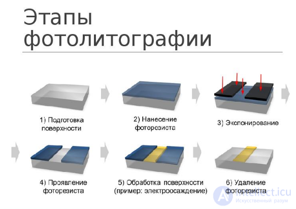
The essence of the photolithography process comes down to the fact that a photoresist is applied to the surface to be treated, which is exposed to light through a photo pattern with a given pattern. Next, the exposed areas of the photoresist are removed in the developer. The pattern obtained on the photoresist is used for such technological stages of planar technology as etching, electrodeposition, vacuum deposition, sandblasting and others. After carrying out one of these processes, the remnants of the photoresist are removed by the snapshot.
The fundamental difference between photolithography and other types of lithography is that exposure is produced by visible or ultraviolet radiation, while other types of lithography use x-ray radiation, electron flow, ion flow, hard ultraviolet, and more.
If there is contamination on the plate, the plate can be washed off in a two-step process: cleaning with acetone, to remove organic contaminants, and then rinsing in isopropanol to remove the remaining acetone. In case of significant contamination of the surface, it can be treated with a solution of H 2 SO 4 and H 2 O 2 , followed by an RCA cleaning process. To clean the surface of water molecules precipitated from the air, the surface is heated to a temperature of about 120 ° C for a few minutes.
Different surfaces have different adhesion, which must be considered in the process of applying a photoresist. For example, metals such as aluminum, chromium and ititan have excellent adhesion, while noble metals such as gold or platinum have very poor adhesion. In case of poor adhesion, before applying the photoresist, first apply a sublayer (adhesive) that enhances adhesion, such as hexamethyldisilazane (HMDS). In addition, sometimes pre-and sometimes over the photoresist, apply anti-reflective coating.
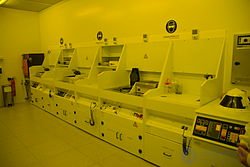
Centrifuging units for photoresist application
The most common method of applying photoresists to the surface is centrifuging. This method allows you to create a uniform film of photoresist and control its thickness plate rotation speed (about several thousand revolutions per minute). It is generally used when working with large round plates.
When using surfaces that are not suitable for centrifuging, for example, to coat small surfaces, dip coating is applied to the photoresist. The disadvantages of this method are the high consumption of photoresist and the heterogeneity of the resulting films.
If necessary, apply a resist on complex surfaces using aerosol spraying, however, the film thickness with this method of application is also not uniform.
After applying the resist, it is necessary to pre-dry it (bristling). For this, the sample is kept for several minutes in a furnace, at a temperature of 100-120 o C. This stage is necessary for evaporation of the solvent contained in the photoresist, which improves adhesion, eliminates sticking to the photo pattern, the possibility of applying the second layer of photoresist and has a positive effect in some other aspects.
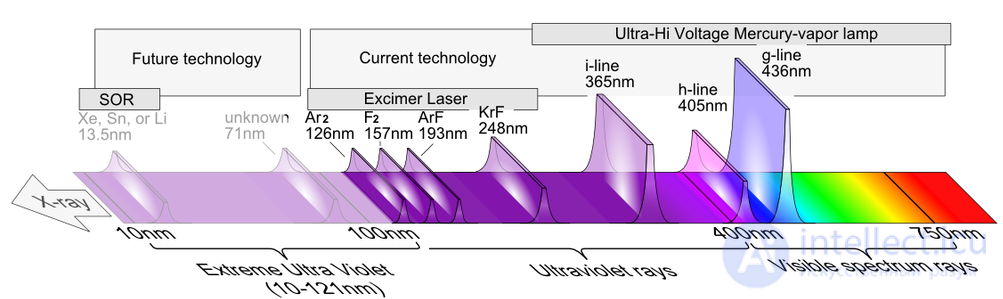
Wavelengths of exposure in lithography
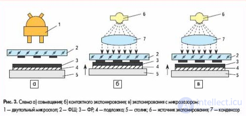
Schemes of 4 different types of exposure. Showing the contact method of exposure, exposure with microgap and projection methods of exposure


The process of exposure is the illumination of the photoresist through a photomask containing the desired pattern, light of the visible or ultraviolet range, which distinguishes the process of photolithography from other types of lithography. For example, in the case of X-ray, ion-beam and electron lithography, X-rays, ions and electrons, respectively, are used for exposure.
The most standard wavelengths of exposure in photolithography are the i-line (365nm), the h-line (405nm) and the g-line (436nm). However, most photoresists can be exposed to a wide spectrum in the ultraviolet range (integral exposure), for which a mercury lamp is usually used. In the case of photolithography in deep (hard) ultraviolet, wavelengths of about 13.5 nm and special photoresists are used. The most common sources of radiation used in photolithography are:
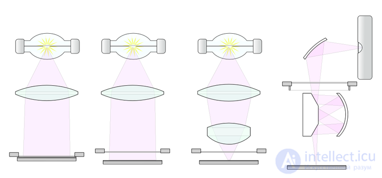
Exposure can be carried out with or without a photomask (maskless lithography). In the latter case, the pattern on the photoresist is formed by a directly moving laser or electron beam or their group focused on the surface of the photoresist. In the case of the use of photomasks, projection methods of exposure are more often used when the pattern from the photomask is transferred to the photoresist using an optical lens system. In some variants of lithography, the mask may be in contact with the photoresist, or in close proximity, in the presence of a microgap.
There are technologies that can reduce distortion and make chips with smaller design standards:
In the production of semiconductor devices, devices such as steppers and scanners, in which a small photomask is exposed to the plate many times by moving the exposed surface, are used to expose plates of large area (150, 200, 300 mm in diameter).
The main parameters of exposure are the wavelength, exposure time and the power of the radiation source. As a rule, each photoresist has a certain dose value (mJ / cm 2 ) necessary for its exposure, so it is important to choose the right exposure parameters. With an insufficient dose, problems with photoresist development can occur, and excessive exposure can cause damage to the photoresist film. The performance of photolithographic installations, measured in plates per hour (wph), depends on the power parameters.
Additionally, it is worth noting such a method of photolithography, as “burning out”, in which the necessary windows in the polymer layer are burned under the influence of a powerful light flux on them, evaporating the film deposited on the material or burning through the material itself. This method is used for the manufacture of short-circuited offset forms and in some systems of risography.
Secondary hardening is performed immediately after exposure and is not a required step. This stage is required only in cases of using chemically enhanced photoresists, applying reversible photoresist, the need for relaxation of thick photoresist films, and in some other situations.
In the process of development, parts of the photoresist are removed with a special developer liquid (for example, tetramethylammonium hydroxide), forming windows in the photoresist film. In the case of using a positive photoresist, the exposed area is removed, and in the case of a negative, not exposed.
Certain photoresists are shown by a certain developer and are not shown by others. As a rule, the developer is diluted with water (1: 2, 1: 4), and the degree of dilution controls the speed of development, which also depends on the dose received by the photoresist during exposure.
The final hardening of the photoresist is also not a necessary step, although it often helps to improve its properties. In particular, drying at 130-140 ° C increases the chemical and temperature resistance of the developed photoresist for such subsequent stages as electrodeposition, dry and liquid etching.
As a rule, photolithography is closely related to the technological stage, for which the figure obtained from photoresist is actually required. The most common process at this stage is etching, although processes such as electrodeposition and sputtering are often used during reverse photolithography.
Etching
Main article: Etching
Etching is the most commonly used process in combination with photolithography, in the manufacture of printed circuit boards and semiconductor devices for microelectronics. There are two main types of etching: liquid (liquid) and plasma (dry). Depending on the tasks, apply one or another type of etching. In general, liquid etching is used mainly in the manufacture of printed circuit boards, as well as for etching the sacrificial layer in the manufacture of MEMS, and other applications that require isotropic etching (i.e. etching in all directions). Plasma, and especially deep plasma etching, is used when it is necessary to etch the structure relatively deeply, while maintaining the vertical angle of inclination of the walls as much as possible, that is, etching anisotropically, only in the vertical direction. The result of etching is closely related to the parameters of the photoresist, which largely determines its choice.
Electrodeposition
In the process of electrodeposition, the windows in the photoresist are used to precipitate material from the electrolyte in them.
Spraying Reverse lithography
In cases when it is required to obtain a drawing from a material that is poorly etched, the process of reverse (explosive) lithography is used. In the process of reverse lithography, a thin layer of material (usually metal) from which you want to form a pattern is sprayed onto the applied and developed photoresist. At the next stage, the photoresist is removed, so that the sprayed material remains only in the windows unprotected by the photoresist, and the film caught on the photoresist is carried along with it, that is, the so-called “explosion” is carried out. For reverse lithography, as a rule, special LOR (lift-of-resist) photoresists are used. There are numerous modifications of this method, for example, when two or even three layers of photoresists are used with different manifestation speeds. In general, for accurate removal of photoresist, it is required that the photoresist film be two or more times thicker than the film of the sprayed material, as well as the walls of the photoresist have a negative slope, which will exclude the possibility of covering them with the sprayed material.
The final stage of the photolithography process is the removal of the photoresist. To remove the photoresist from the treated surface, a special extracting liquid (for example, dimethyl sulfoxide) is used. As a rule, certain shooters are suitable only for certain groups of photoresists. In the process of reverse photolithography, together with the photoresist, the material film covering it is also removed. If at the previous stages adhesion enhancers or anti-release coatings were used, they are usually also removed by the remover.
there are other methods

Comments
To leave a comment
Design and engineering of electronic equipment
Terms: Design and engineering of electronic equipment