Lecture
In the overwhelming majority of cases, each of the switching planes, the number of which corresponds to the number of conducting layers, is considered as Cartesian with grid spacing determined by the type of board and installed by the IET. Conductors should be diluted successively one after the other before laying the last route or establishing the fact that it is impossible to lay the next one with a given number of conductive layers.
Direct wiring, which allows traces along the shortest path, leads to a rapid complication of the conductive pattern, an unjustified increase in the number of conductive layers, and is justified by simple modules with variable-size IET or ultrahigh-speed modules, where the minimum connection length is of fundamental importance.
The coordinate method allows for the location of conductors only parallel to one of the coordinate axes, i.e., a line of arbitrary direction is replaced with a broken line of orthogonal etrezks in different layers connected by transition or mounting holes. The orthogonal arrangement of conductors in adjacent layers reduces parasitic connections, organizes tracing and facilitates automation of its execution, but increases the length of traces (up to 1.42 times).
The electrophysical and operational characteristics of metallized vias are worse than those of printed conductors. The number of vias can be significantly reduced, if you allow the runs at an angle of 45 ° to the grid lines. This allows for shifts and successive turns of the direction of the tracks, which are necessary when walking around contact pads and other obstacles, without resorting to interlayer transitions.
The choice of the sequence of distributing conductors largely determines the complexity and quality of the trace. A wiring variant is used, in which the wiring of power supply lines and zero potential is performed first, and then they proceed to a trace by the above method. In simple analog REFUs, wiring according to an electrical circuit is justified, when all connections connected to the first IC (cascade) are performed, then to the second, and so on.
With any method of wiring with an increase in the number of already divorced conductors, the trace becomes more complicated, and it is possible that the following connection with a given number of layers is impossible or requires a complex and lengthy path. In this case, a review of the decisions already taken and an iterative change in the trace are necessary.
For the convenience of developing a conductive pattern, the entire set of transmission lines is divided into two groups: signal, the main purpose of which is to transmit signals with distortions that are less acceptable; potential — power supplies and zero potential.
GENERAL CONSIDERATIONS
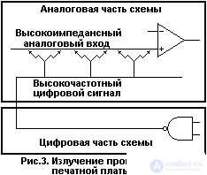
Due to the significant differences between analog circuitry and digital circuitry, the analog part of the circuit must be separated from the rest, and its wiring must follow special methods and rules. The effects arising from the imperfect characteristics of printed circuit boards become especially noticeable in high-frequency analog circuits, but the general form errors described in this article can affect the quality characteristics of devices operating even in the audio frequency range.
The intention of this article is to discuss common mistakes made by the developers of printed circuit boards, a description of the impact of these errors on quality indicators and recommendations for solving the problems encountered.
The circuit board is a component of the circuit.
Only in rare cases, the circuit board of an analog circuit can be diluted so that its effects do not have any influence on the operation of the circuit. At the same time, any such impact can be minimized so that the characteristics of the analog circuit of the device are the same as those of the model and the prototype.
Layout
Developers of digital circuits can correct small errors on the manufactured board, complementing it with jumpers or, conversely, removing unnecessary conductors, making changes to the operation of programmable chips, etc., moving very soon to the next development. For an analog circuit this is not the case. Some of the common mistakes discussed in this article cannot be fixed by adding jumpers or removing extra conductors. They can and will render the entire PCB inoperative.
It is very important for a digital designer who uses such remedies to read and understand the material outlined in this article well in advance of the project’s transfer to production. A little attention paid during development and a discussion of possible options will help not only prevent the PCB from becoming waste, but also reduce the cost due to blunders in a small analog part of the circuit. Finding errors and fixing them can result in losses of hundreds of hours. Layout can reduce this time to one day or less. Make all your analog circuits.
Sources of noise and interference
Noise and interference are the main elements that limit the quality characteristics of the circuits. Interference can both be emitted by sources and also be induced by circuit elements. An analog circuit is often located on a printed circuit board along with high-speed digital components, including digital signal processors ( DSP ).
High-frequency logic signals create significant radio frequency interference ( RFI ). The number of sources of noise emission is enormous: key power sources for digital systems, mobile phones, radio and television, power sources for fluorescent lamps, personal computers, lightning, etc. Even if the analog circuit operates in the audio frequency range, radio frequency interference can create noticeable noise in the output signal.
PCB CATEGORIES
The choice of PCB design is an important factor in determining the mechanical characteristics when using the device as a whole. For the manufacture of printed circuit boards used materials of different levels of quality. The most suitable and convenient for the developer will be if the manufacturer of printed circuit boards is nearby. In this case, it is easy to control the resistivity and the dielectric constant - the main parameters of the material of the printed circuit board. Unfortunately, this is not enough and it is often necessary to know other parameters, such as flammability, high temperature stability and hygroscopicity coefficient. These parameters can be known only by the manufacturer of the components used in the manufacture of printed circuit boards.
Laminates are designated with FR ( flame resistant, flame retardant ) and G indexes. The material with the FR-1 index is the most flammable and the FR-5 is the least flammable . Materials with indexes G10 and G11 have special characteristics. Materials printed circuit boards are given in Table. one.
Do not use the FR-1 category PCB. There are many examples of the use of FR-1 printed circuit boards, which are damaged by heat from powerful components. Printed circuit boards in this category are more like cardboard.
FR-4 is often used in the manufacture of industrial equipment, while FR-2 is used in the manufacture of household appliances. These two categories are industry standardized, and the FR-2 and FR-4 printed circuit boards are often suitable for most applications. But sometimes the imperfection of the characteristics of these categories leads to the use of other materials. For example, for very high frequency applications, fluoroplastic and even ceramics are used as printed circuit board material. However, the more exotic the PCB material, the higher the price can be.
When choosing a printed circuit board material, pay special attention to its hygroscopicity, since this parameter can have a strong negative effect on the desired characteristics of the board - surface resistance, leakage, high-voltage insulating properties (breakdowns and sparks) and mechanical strength. Also pay attention to the operating temperature. High temperature areas may occur in unexpected places, such as near large digital integrated circuits that switch at high frequency. If such areas are located directly below the analog components, the temperature increase may affect the characteristics of the analog circuit.
Table 1
|
Category |
Components, comments |
|
FR-1 |
paper, phenolic composition: pressing and stamping at room temperature, high hygroscopicity coefficient |
|
FR-2 |
paper, phenolic composition: applicable for one-sided printed circuit boards of household appliances, low coefficient of hygroscopicity |
|
FR-3 |
paper, epoxy composition: developments with good mechanical and electrical characteristics |
|
FR-4 |
fiberglass, epoxy composition: excellent mechanical and electrical properties |
|
FR-5 |
fiberglass, epoxy composition: high strength at elevated temperatures, no ignition |
|
G10 |
fiberglass, epoxy composition: high insulating properties, the highest strength glass fiber, low coefficient of hygroscopicity |
|
G11 |
fiberglass, epoxy composition: high bending strength at elevated temperatures, high solvent resistance |
After the material of the printed circuit board is selected, it is necessary to determine the thickness of the foil of the printed circuit board. This parameter is primarily selected based on the maximum amount of current flowing. If possible, try to avoid using very thin foils.
NUMBER OF PCB LAYERS
Depending on the total complexity of the scheme and quality requirements, the developer must determine the number of layers of the printed circuit board.
Single layer printed circuit boards
Very simple electronic circuits are carried out on one-sided boards using low-cost foil materials (FR-1 or FR-2) and often have many jumpers, resembling double-sided boards. This method of creating printed circuit boards is recommended only for low-frequency circuits. For reasons that will be described below, one-sided printed circuit boards are heavily susceptible to interference . A good one-sided PCB is difficult to develop because of many reasons. Nevertheless, good boards of this type are found, but when developing them, a lot of things need to be thought out in advance.
Double Layer PCB
At the next level, there are two-sided printed circuit boards, which in most cases use FR-4 as the substrate material, although FR-2 is sometimes found. The use of FR-4 is more preferable, since the holes in the printed circuit boards from this material are of better quality. Schemes on double-sided printed circuit boards are divorced much easier, because in two layers it is easier to carry out the layout of intersecting tracks. However, for analog circuits, the intersection of the tracks is not recommended. Where possible, the bottom layer ( bottom ) should be taken under the landfill, and the rest signals should be spread in the top layer ( top ). Using the landfill as a ground tire provides several advantages:
Despite their advantages, double-sided printed circuit boards are not the best, especially for low-signal or high-speed circuits. In general, the thickness of the PCB, i.e. the distance between the metallization layers is 1.5 mm, which is too much to fully realize some of the advantages of the two-layer printed circuit board listed above. Distributed capacity, for example, is too small due to such a large interval.
Multilayer printed circuit boards
For responsible circuit design requires multilayer printed circuit boards (WFP). Some reasons for their use are obvious:
In addition to these reasons for the use of multilayer printed circuit boards, there are other, less obvious:
The order of the layers
Inexperienced developers often have some confusion about the optimal order of the layers of the printed circuit board. Take for example a 4-layer chamber containing two signal layers and two polygon layers - the earth layer and the power layer. What is the best layer order? Signal layers between polygons that will serve as screens? Or make the polygon layers internal to reduce the interference of the signal layers?
When solving this issue, it is important to remember that often the arrangement of the layers does not matter much, since all the same the components are located on the outer layers, and the tires bringing signals to their conclusions sometimes pass through all the layers. Therefore, any screen effects are only a compromise. In this case, it is better to take care of creating a large distributed capacity between the food and land polygons, placing them in the inner layers.
Another advantage of the location of the signal layers outside is the availability of signals for testing, as well as the possibility of modifying connections. Anyone who has ever changed connections of conductors located in the inner layers will appreciate this possibility.
For printed circuit boards with more than four layers, there is a general rule to place high-speed signal conductors between the ground and power polygons, and low-frequency conductors for outer layers.
GROUNDING
Good grounding is a common requirement for a rich, multi-layered system. And it should be planned from the first step of the design development.
The main rule: the division of land .
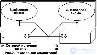
Dividing the land into analog and digital parts is one of the simplest and most effective noise reduction methods. One or more layers of a multi-layer printed circuit board is usually retracted below the ground layer. If the developer is not very experienced or inattentive, then the land of the analog part will be directly connected to these polygons, i.e. analog return current will use the same circuit as digital return current. Auto distributors work in a similar way and combine all the lands together.
If a previously developed printed circuit board with a single earth ground uniting analog and digital lands is recycled, then you must first physically divide the lands on the board (after this operation, the board becomes almost impossible). After that, all connections to the analog earth ground of the analog circuit components (analog ground are formed) and to the digital earth ground of the digital circuit components (digital earth is formed) are produced. And only after this, the source combines digital and analog earth.
Other land formation rules:
Почти все сигналы тактовых частот являются достаточно высокочастотными сигналами, поэтому даже небольшие емкости между трассами и полигонами могут создавать значительные связи. Необходимо помнить, что не только основная тактовая частота может вызывать проблему, но и ее высшие гармоники.
Пример хорошего размещения компонентов
На рисунке 4 показан возможный вариант размещения всех компонентов на плате, включая источник питания. Здесь используются три отделенных друг от друга и изолированных полигона земли/питания: один для источника, один для цифровой схемы и один для аналоговой. Цепи земли и питания аналоговой и цифровой частей объединяются только в источнике питания. Высокочастоный шум отфильтровывается в цепях питания дросселями. В этом примере высокочастотные сигналы аналоговой и цифровой частей отнесены друг от друга. Такой дизайн имеет очень высокую вероятность на благоприятный исход, поскольку обеспечено хорошее размещение компонентов и следование правилам разделения цепей.
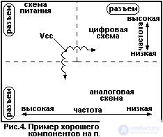
Имеется лишь один случай, когда необходимо объединение аналоговых и цифровых сигналов над областью полигона аналоговой земли. Аналого-цифровые и цифро-аналоговые преобразователи размещаются в корпусах с выводами аналоговой и цифровой земли. Принимая во внимание предыдущие рассуждения, можно предположить, что вывод цифровой земли и вывод аналоговой земли должны быть подключенны к шинам цифровой и аналоговой земли соответственно. Однако в данном случае это не верно.
Названия выводов (аналоговый или цифровой) относятся лишь к внутренней структуре преобразователя, к его внутренним соединениям. В схеме эти выводы должны быть подключены к шине аналоговой земли. Соединение может быть выполнено и внутри интегральной схемы, однако получить низкое сопротивление такого соединения довольно сложно из-за топологических ограничений. Поэтому при использовании преобразователей предполагается внешнее соединение выводов аналоговой и цифровой земли. Если этого не сделать, то параметры микросхемы будут значительно хуже приведенных в спецификации.
Необходимо учитывать то, что цифровая элементы преобразователя могут ухудшать качественные характеристики схемы, привнося цифровые помехи в цепи аналоговой земли и аналогового питания. При разработке преобразователей учитывается это негативное воздействие так, чтобы цифровая часть потреб***яла как можно меньше мощности. При этом помехи от переключений логических элементов уменьшаются. Если цифровые выводы преобразователя не сильно нагружены, то внутренние переключения обычно не вызывают особых проблем. При разработке печатной платы, содержащей АЦП или ЦАП, необходимо должным образом отнестись к развязке цифрового питания преобразователя на аналоговую землю.
ЧАСТОТНЫЕ ХАРАКТЕРИСТИКИ ПАССИВНЫХ КОМПОНЕНТОВ
Для правильной работы аналоговых схем весьма важен правильный выбор пассивных компонентов. Начинайте дизайнерскую разработку с внимательного рассмотрения высокочастотных характеристик пассивных компонентов и предварительного размещения и компоновки их на эскизе платы.
Большое число разработчиков совершенно игнорируют частотные ограничения пассивных компонентов при использовании в аналоговой схемотехнике. Эти компоненты имеют ограниченные частотные диапазоны и их работа вне специфицированной частотной области может привести к непредсказуемым результатам. Кто-то может подумать, что это обсуждение касается только высокоскоростных аналоговых схем. Однако, это далеко не так - высокочастотные сигналы достаточно сильно воздействуют на пассивные компоненты низкочастотных схем посредством излучения или прямой связи по проводникам. Например, простой низкочастотный фильтр на операционном усилителе может легко превращаться в высокочастотный фильтр при воздействии на его вход высокой частоты.
Резисторы
Высокочастотные характеристики резисторов могут быть представлены эквивалентной схемой, приведенной на рисунке 5.

Обычно применяются резисторы трех типов: 1) проволочные, 2) углеродные композитные и 3) пленочные. Не надо иметь много воображения, чтобы понять, как проволочный резистор может превращаться в индуктивность, поскольку он представляет собой катушку с проводом из высокоомного металла. Большинство разработчиков электронных устройств не имеют понятия о внутренней структуре пленочных резисторов, которые также представляют собой катушку, правда, из металлической пленки. Поэтому пленочные резисторы также обладают индуктивностью, которая меньше, чем у проволочных резисторов. Пленочные резисторы с сопротивлением не более 2 кОм можно свободно использовать в высокочастотных схемах. Выводы резисторов параллельны друг другу, поэтому между ними существует заметная емкостная связь. Для резисторов с большим сопротивлением межвыводная емкость будет уменьшать полный импеданс на высоких частотах.
Конденсаторы
Высокочастотные характеристики конденсаторов могут быть представлены эквивалентной схемой, приведенной на рисунке 6.
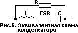
Конденсаторы в аналоговых схемах используются в качестве элементов развязки и фильтрующих компонентов. Для идеального конденсатора реактивное сопротивление определяется по следующей формуле:
Следовательно, электролитический конденсатор емкостью 10 мкФ будет обладать сопротивлением 1,6 Ом на частоте 10 кГц и 160 мкОм на частоте 100 МГц. Is it so?
В действительности, никто никогда не видел электролитического конденсатора с реактивным сопротивлением 160 мкОм. Обкладки пленочных и электролитических конденсаторов представляют собой свитые слои фольги, которые создают паразитную индуктивность. Эффект собственной индуктивности у керамических конденсаторов значительно меньше, что позволяет использовать их при работе на высоких частотах. Кроме этого, конденсаторы обладают током утечки между обкладками, который эквивалентен включенному параллельно их выводам резистору, добавляющему свое паразитное воздействие к воздействию последовательно включенного сопротивления выводов и обкладок. К тому же, электролит не является идеальным проводником. Все эти сопротивления складываясь создают эквивалентное последовательное сопротивление ( ESR ). Конденсаторы, используемые в качестве развязок должны обладать малым ESR, поскольку последовательное сопротивление ограничивает эффективность подавления пульсаций и помех. Повышение рабочей температуры довольно значительно увеличивает эквивалентное последовательное сопротивление и может привести к ухудшению характеристик конденсатора. Поэтому, если предполагается использование алюминиевого электролитического конденсатора при повышенной рабочей температуре, то необходимо использовать конденсаторы соответствующего типа (105°С).
Выводы конденсатора также вносят свой вклад в увеличение паразитной индуктивности. Для малых значений емкости важно оставлять длину выводов короткой. Сочетание паразитных индуктивности и емкости может создать резонансный контур. Полагая, что выводы имеют индуктивность порядка 8 нГн на один сантиметр длины, конденсатор емкостью 0,01 мкФ с выводами длиной по одному сантиметру будет иметь резонансную частоту около 12,5 МГц. Этот эффект известен инженерам, которые десятилетия назад разрабатывали электронные вакуумные приборы. Тот, кто восстанавливает антикварные радиоприемники и не знает об этом эффекте, сталкивается с множеством проблем.
При использовании электролитических конденсаторов необходимо следить за правильным подключением. Положительный вывод должен быть подключен к более положительному постоянному потенциалу. Неправильное подключение приводит к протеканию через электролитический конденсатор постоянного тока, что может вывести из строя не только сам конденсатор, но и часть схемы.
В редких случаях разность потенциалов по постоянному току между двумя точками в схеме может менять свой знак. Это требует применения неполярных электролитических конденсаторов, внутренняя структура которых эквивалентна двум полярным конденсаторам, соединенным последовательно.
Индуктивности
Высокочастотные характеристики индуктивностей могут быть представлены эквивалентной схемой, приведенной на рисунке 7.
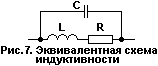
Реактивное сопротивление индуктивности описывается следующей формулой:
Следовательно, индуктивность 10 мГн будет обладать реактивным сопротивлением 628 Ом на частоте 10 кГц, а на частоте 100 МГц - сопротивлением 6,28 МОм. Right?
In fact, there is no inductance with a reactance of 6.28 MΩ. The nature of the parasitic resistance is easy to understand - the turns of the coil are made of wire, which has some resistance per unit length. The parasitic capacitance is perceived more difficult until it is taken into account that the next turn of the coil is located close to the previous one, and a capacitive coupling occurs between closely spaced conductors. Parasitic capacitance limits the upper operating frequency. Small wire inductances begin to become inefficient in the range of 10 ... 100 MHz.
Printed circuit board
The printed circuit board itself has the characteristics of the passive components discussed above, but not so obvious.
The pattern of conductors on a printed circuit board can be both a source and receiver of interference. Good wiring of conductors reduces the sensitivity of the analog circuit to the radiation sources.
A printed circuit board is susceptible to radiation, since the conductors and the terminals of the components form peculiar antennas. The theory of antennas is a fairly complex subject to study and is not covered in this article. However, some basics are provided here.
A bit of antenna theory
One of the main types of antennas is a pin or straight conductor. This antenna works because the direct conductor has a parasitic inductance and therefore can concentrate and pick up radiation from external sources. The full impedance of a direct conductor has resistive (active) and inductive (reactive) components:

At a direct current or low frequencies the active component prevails. With increasing frequency, the reactive component becomes more and more significant. In the range from 1 kHz to 10 kHz, the inductive component begins to influence, and the conductor is no longer a low-impedance connector, but rather acts as an inductor.
The formula for calculating the inductance of a conductor of a printed circuit board is as follows:
Typically, tracks on a printed circuit board have values from 6 nH to 12 nH per centimeter length. For example, a 10-centimeter conductor has a resistance of 57 mΩ and an inductance of 8 nH / cm. At a frequency of 100 kHz, the reactance becomes 50 mΩ, and at higher frequencies the conductor will be inductance rather than active resistance.
The rule of the whip antenna states that it begins to interact noticeably with the field at its length of about 1/20 of the wavelength, and the maximum interaction occurs at the length of the pin equal to 1/4 of the wavelength. Therefore, the 10 cm wire from the example in the previous paragraph will start to become a pretty good antenna at frequencies above 150 MHz. It must be remembered that despite the fact that the clock of the digital circuit may not work at a frequency above 150 MHz, there are always higher harmonics in its signal. If the PCB contains components with pin pins of considerable length, then these pins can also serve as antennas.
Another main type of antenna is loopback antenna. The inductance of a straight conductor increases greatly when it bends and becomes part of the arc. Increasing inductance lowers the frequency at which the antenna begins to interact with the field lines.
Experienced PCB designers, who are well versed in the theory of loop antennas, know that you cannot create loops for critical signals. Some developers, however, do not think about it, and the conductors of the return and signal current in their circuits are loops. Creating loopback antennas is easy to show with an example (Fig. 8). In addition, the creation of a slot antenna is shown here.
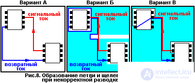
Consider three cases:
Option A is an example of bad design. It does not use the analog ground polygon at all. The loop loop is formed by the earth and signal conductor. With the passage of current, electric and perpendicular magnetic fields arise. These fields form the basis of a loopback antenna. The rule of a loopback antenna states that for maximum efficiency, the length of each conductor should be equal to half the wavelength of the received radiation. However, it should be remembered that even at 1/20 of the wavelength, the loop antenna is still quite effective.
Option B is better than option A, but there is a gap in the landfill, probably to create a specific place for the wiring of the signal conductors. Paths of signal and return currents form a slot antenna. Other loops are formed in the cutouts around the microcircuits.
Option B is an example of better design. The signal and return current paths are the same, negating the efficiency of the loop antenna. Note that in this version there are also cuts around the microcircuits, but they are separated from the return current path.
The theory of reflection and matching of signals is close to the theory of antennas.
When the conductor of the circuit board rotates through a 90 ° angle, a signal reflection may occur. This is mainly due to a change in the width of the current path. At the apex of the corner, the width of the path increases 1.414 times, which leads to a mismatch of the characteristics of the transmission line, especially the distributed capacitance and the own inductance of the path. Quite often it is necessary to rotate the circuit by 90 ° on the PCB. Many modern CAD-packages allow you to smooth the corners of the runs or to trace the tracks in the form of an arc. Figure 9 shows two steps to improve the shape of the angle. Only the last example maintains a constant width of the path and minimizes reflections.
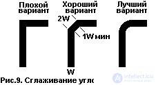
Tip for experienced PCB distributors: leave the smoothing procedure to the last stage of work before creating droplet-shaped leads and filling polygons. Otherwise, the CAD package will take longer to smooth due to more complex calculations.
PARASITIC EFFECTS OF THE PCB
Capacitive coupling occurs when the conductors of a printed circuit board are on different layers when they intersect. Sometimes this can create a problem. Conductors placed on top of each other on adjacent layers create a long film capacitor. The capacitance of such a capacitor is calculated by the formula given in figure 10.
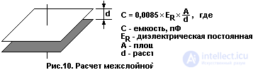
For example, a printed circuit board may have the following parameters:
- 4 layers; the signal and land layer of the land are adjacent,
- interlayer spacing - 0.2 mm,
- conductor width - 0.75 mm,
- conductor length - 7.5 mm.
The typical value of the dielectric constant ER for FR-4 is 4.5.
Substituting all the values in the formula, we obtain the value of the capacitance between these two tires, equal to 1.1 pF. Even such a seemingly small capacity is unacceptable for some applications. Figure 11 illustrates the effect of a 1 pF capacitance when it is connected to the inverting input of a high-frequency operational amplifier.
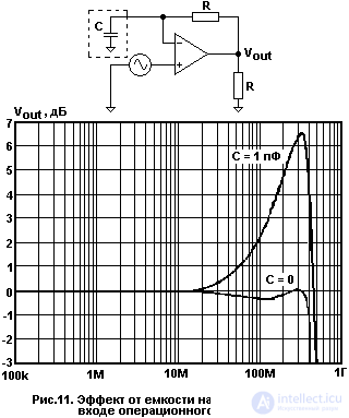
It is seen that there is a doubling of the amplitude of the output signal at frequencies close to the upper limit of the frequency range of the shelter. This, in turn, can lead to generation, especially at the operating frequencies of the antenna (above 180 MHz).
This effect gives rise to numerous problems, to solve which, however, there are many ways. The most obvious of these is the reduction in the length of the conductors. Another way is to reduce their width. There is no reason to use a conductor of this width for connecting the signal to the inverting input, since a very small current flows through this conductor. Reducing the length of the track to 2.5 mm, and width to 0.2 mm will lead to a decrease in capacitance to 0.1 pF, and such a capacity will not lead to such a significant increase in frequency response. Another solution is to remove part of the polygon under the inverting input and the conductor that is suitable for it.
The inverting input of an operational amplifier, especially a high-speed amplifier, is largely prone to generation in high gain circuits. This is due to the undesirable capacity of the input stage of the OU. Therefore, it is extremely important to reduce the parasitic capacitance and position the feedback components as close to the inverting input as possible. If, despite the measures taken, the amplifier is excited, it is necessary to proportionally reduce the resistance of the feedback resistors to change the resonant frequency of the circuit. An increase in resistors can also help, though much less frequently, since the excitation effect depends on the circuit impedance. When changing the feedback resistors, we should not forget about the change in the capacitance of the correction capacitor. Also, we should not forget that when the resistance of resistors decreases, the power consumption of the circuit *** increases.
The width of the conductors of the PCB can not be infinitely reduced. The maximum width is determined by both the process and the thickness of the foil. If two conductors pass close to each other, then a capacitive and inductive coupling is formed between them (Fig. 12).
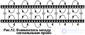
The dependencies that describe these parasitic effects are complex enough to result in this article, but they can be found in the literature on transmission lines and strip lines.
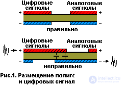
Signal conductors should not be run parallel to each other, except when wiring differential or microstrip lines. The gap between the conductors must be at least three times the width of the conductors.
The capacitance between the tracks in analog circuits can create difficulties with large resistances of resistors (several MOhm). The relatively large capacitive coupling between the inverting and non-inverting inputs of the operational amplifier can easily lead to self-excitation of the circuit.
Whenever when wiring a printed circuit board there is a need to create a via, i.e. interlayer connection (Fig. 13), it must be remembered that this also gives rise to parasitic inductance. When the diameter of the hole after metallization d and the length of the channel h inductance can be calculated by the following approximate formula:
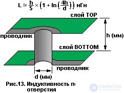
For example, when d = 0.4 mm and h = 1.5 mm (fairly common values), the inductance of the hole is 1.1 nH.
Keep in mind that the inductance of the hole together with the same parasitic capacitance form a resonant circuit, which can affect when working at high frequencies. The self-inductance of the hole is rather small, and the resonant frequency is somewhere in the gigahertz range, but if the signal is forced to pass through several vias during its path, then their inductances are added (series connection), and the resonant frequency decreases. Conclusion: try to avoid a large number of vias when wiring critical high-frequency conductors of analog circuits . Another negative phenomenon: with a large number of vias in the landfill, loopbacks can be created. The best analog wiring - all signal conductors are located on one layer of the printed circuit board.
In addition to the parasitic effects discussed above, there are also those that are associated with an insufficiently clean surface of the board.
Remember that if there are large resistances in the circuit, then special attention should be paid to cleaning the board. At the final manufacturing operations of the printed circuit board, flux and dirt residues should be removed. Recently, when installing printed circuit boards, water-soluble fluxes are often used. Being less harmful, they are easily removed with water. But at the same time, washing the board with insufficiently clean water can lead to additional contaminations that impair the dielectric characteristics. Therefore, it is very important to wash the circuit board with a high-impedance circuit with fresh distilled water.
SIGNAL DISCHARGE
As already noted, interference can penetrate into the analog part of the circuit through the power supply circuit. To reduce such interference, decoupling (blocking) capacitors are used, reducing the local impedance of the power supply bus.
If it is necessary to dissolve a printed circuit board, on which there are both analog and digital parts, then it is necessary to have at least a small understanding of the electrical characteristics of the logic elements.
A typical output cascade of a logic element contains two transistors connected in series with each other, as well as between the power supply and ground circuits (Fig. 14).
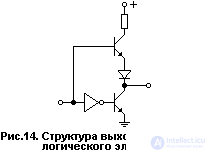
In the ideal case, these transistors operate strictly in antiphase, i.e. when one of them is open, at the same time the second is closed, forming at the output either a signal of a logical unit or a logical zero. In the steady-state logical state, the power consumption of the logic element is small.
The situation changes dramatically when the output stage switches from one logical state to another. In this case, for a short period of time, both transistors can be opened simultaneously, and the power supply current of the output stage increases greatly as the resistance of the current path section from the power bus to the earth bus through two series-connected transistors decreases. Power consumption increases abruptly, and then also decreases, which leads to a local change in the supply voltage and the appearance of a sharp, short-term change in current. Such changes in current lead to the emission of radio frequency energy. Even on a relatively simple printed circuit board there may be dozens or hundreds of considered output stages of logic elements, therefore the total effect of their simultaneous operation can be very large.
It is impossible to accurately predict the range of frequencies in which these current surges will be located, since the frequency of their occurrence depends on many reasons, including the propagation delay of switching transistors of a logic element. The delay, in turn, also depends on many random reasons arising during the production process. The switching noise has a wideband distribution of harmonic components over the entire range. There are several ways to suppress digital noise, the use of which depends on the spectral distribution of noise.
Table 2 presents the maximum operating frequencies for common types of capacitors.
table 2
|
Type of |
Maximum frequency |
|
aluminum electrolytic |
100 kHz |
|
tantalum electrolytic |
1 MHz |
|
mica |
500 MHz |
|
ceramic |
1 GHz |
From the table it is obvious that tantalum electrolytic capacitors are used for frequencies below 1 MHz, at higher frequencies ceramic capacitors should be used. It must be remembered that capacitors have their own resonance and their wrong choice can not only help but exacerbate the problem. Figure 15 shows typical intrinsic resonances of two general-purpose capacitors — 10 μF of tantalum electrolytic and 0.01 μF of ceramic.
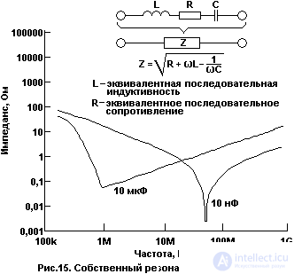
Actual characteristics may differ from different manufacturers and even from batch to batch from one manufacturer. It is important to understand that in order for the capacitor to work effectively, the frequencies it suppresses must be in a lower range than the frequency of its own resonance. Otherwise, the nature of the reactance will be inductive, and the capacitor will stop working efficiently.
Do not be mistaken about the fact that one 0.1 μF capacitor will suppress all frequencies. Small capacitors (10 nF and less) can operate more efficiently at higher frequencies.
Isolation of power IC
Isolating the power supply of integrated circuits to suppress high-frequency noise consists in using one or more capacitors connected between the power and ground terminals. It is important that the conductors connecting the leads to the capacitors are short. If this is not the case, then the own inductance of the conductors will play a noticeable role and negate the benefits of using decoupling capacitors.
The decoupling capacitor must be connected to each chip package, regardless of how many operational amplifiers are inside the case — 1, 2, or 4. If the op-amp is powered by a bipolar power supply, then it goes without saying that the decoupling capacitors should be located at each power lead. The capacitance value must be carefully selected depending on the type of noise and interference present in the circuit.
In particularly complex cases, it may be necessary to add an inductance connected in series with the power supply. Inductance must be located before and not after the capacitors.
Другим, более дешевым способом является замена индуктивности резистором с малым сопротивлением (10...100
продолжение следует...
Часть 1 Printed wiring rules
Часть 2 - Printed wiring rules

Comments
To leave a comment
Design and engineering of electronic equipment
Terms: Design and engineering of electronic equipment