Lecture
The file used in the production of the board is created by the developer on the basis of the electrical circuit of the module, requirements for the design of the board and other items of the technical specification. The development of the board is carried out in specialized software packages and produced on a personal computer.
The dimensions of the board must comply with the following requirements of GOST: the multiplicity of length and width is 2.5 mm with the length of the board up to 100 mm, the multiplicity of the length and width of the board is 5 mm with the length of the board up to 350 mm, the multiplicity of length and width with length more than 350 mm, the maximum size is any from the sides no more than 470 mm, the ratio of length to width no more than 3: 1. If the printed circuit board has a non-rectangular shape, then the length of each side must meet the requirements outlined above. In accordance with the chosen dimensions, the contour of the future board is displayed in a specialized graphics editor included in the board development package and is written to the file of the board under development.
The electrical circuit of the development in progress can be transformed into a conductive board pattern in various ways. If the circuit placed on the board contains 3-5 components, then it is more convenient using the graphical tools of the printed circuit board editor to connect the components with manual conductors. With this approach, you can save the developer time spent on drawing the electrical circuit in the circuit editor included in the board development package.
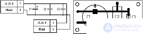
Scheme and power filter board developed in manual mode.
If the scheme is more complicated, then it needs to be transformed into a conductive board pattern in semi-automatic mode. To do this, the circuit will have to be completely drawn in the schematic editor and translated into a set of electrical conductors in a special program.
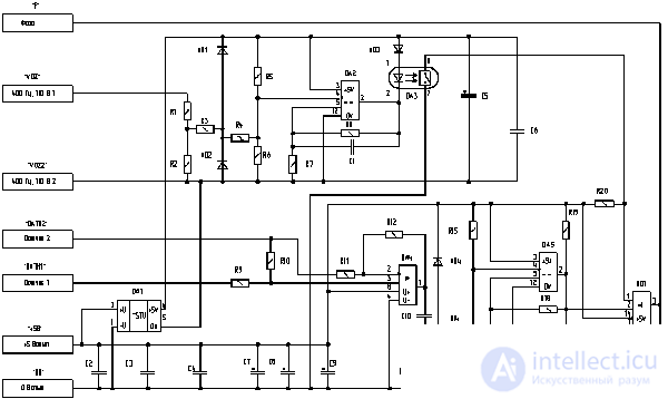
Circuit requiring semi-automatic board development mode.
The board file before starting the transfer of information from the electrical circuit contains the outline of the board in accordance with the required dimensions. Immediately after the data is transferred from the circuit to the board, the developer sees the case of the elements, the outputs of which are connected by lines, indicating electrical connections.
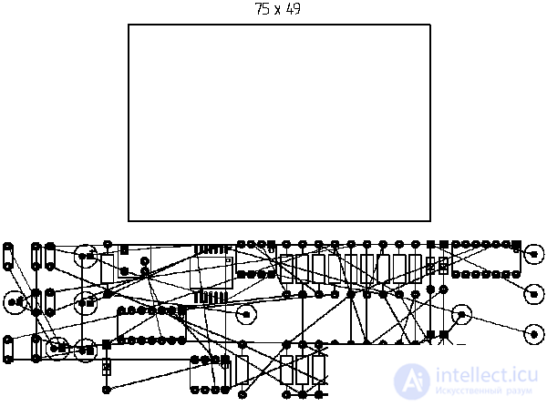
The result of converting the circuit into information for the development of the board.
Replacing the lines with conductive paths, the developer creates a conductive pattern of the board. From the skill of the developer depends on the optimal location of the components on the board, eliminating the intersection and providing the shortest length of conductive tracks. In the development of the card uses data about the components. Conditional graphic designation of the component of the circuit, drawing of the case and information about the conclusions, information about the type of the element body: output or planar, diameters of the holes for installation of the component and dimensions of the mounting pad are included in the component data group. If there are several elements in one case, for example, a resistor array, a dual operational amplifier, and logic elements in one chip, then this information is entered into a data group. In accordance with the type of component, a data group is assigned a name. Information about each component can be stored in a separate file, the name of which corresponds to the type of component or can be combined into several databases: a chip base, a capacitor base, and others.
Often, several newer components are used in the design. For them, the designer independently creates new groups of data. Component databases provided on the Internet or distributed by foreign manufacturers of components contain designations that do not meet the requirements of GOST. Creating a set of documentation using borrowed data about components for designing circuits and boards is impossible. The advantage of the software package for designing boards over drawing packages is that you can get not only the PCB file for production, but also the electrical circuitry included in the design documentation package. Graphic information for drawings of the board can be obtained in a draft that requires further design according to the drawing rules. Therefore, the developer is constantly expanding its own database of components, working on the correctness and completeness of the accumulated information, which allows you to truly automate the development process. The rigid connection between all the information included in a group of data about a single component allows you to eliminate errors, edit, and save developer time when you re-apply components.
Component side of the designed board.
Elements of a conductive pattern, in addition to screens, ground tires, terminal printed contacts and technological printed conductors, are recommended to be located at a distance from the edge not less than the thickness of the printed circuit board, taking into account the tolerance on the dimensions of the sides. It is recommended to use no more than three sizes of mounting and vias. Sites, denoting the first output component, make a different form, different from the rest. For a copper conductor with a thickness of 35 microns and a width of 1 mm with an overheating of 20 degrees, the maximum load capacity is 3 amperes. The maximum current should be reduced by 15% for a distance between conductors equal to or less than their width.
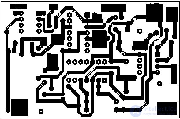
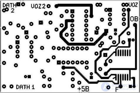
Soldering side of the developed board.
The two sides of the board, the location of the holes and the dimensions of the board are included in one file used in the production of a photomask, drilling holes and milling the outline of the board.
Integration, performance and functionality of electronic systems is constantly growing. Reducing the price and increasing consumer properties leads to increased miniaturization of the element base and an increase in the density of installation on the boards. This is possible thanks to the continuous development of the board production technology. Increasingly, microcircuits are mounted in housings with a large number of pins and a reduced pitch between pins. The practice of electronics production almost everywhere entered the technology of surface mounting. All this led to the formulation of new requirements for the accuracy of manufacturing boards. Along with the most advanced electronics products, the production of devices mastered many years ago is continuing due to the inability of the customer to finance the deep modernization of outdated equipment. The industry produces electronics belonging to different epochs, and sometimes progressive modern solutions in one enterprise coexist with the developments of the past decades. This leads to the existence of different requirements for the accuracy of manufacturing boards, called classes.
The older the class number, the higher the manufacturing accuracy. The class includes descriptions of the requirements for the size of the conductive pattern. The width of the conductor implies the minimum guaranteed width, which the manufacturer undertakes to implement in a conductive pattern with a guarantee of quality.
The width of the minimum conductor in accordance with the accuracy class.
Accuracy class | one | 2 | 3 | four | five |
Minimum conductor width, mm | 0.75 | 0.45 | 0.25 | 0.15 | 0.1 |
Also in the class description is the requirement for the least possible distance between the conductors without short circuits. Due to the manufacturer’s technology, the board produced according to the required class does not have any closures, despite the proximity of the conductors, for example, when producing boards of class 5 with distances between conductors of 0.1 mm and more, the closures are excluded.
The minimum allowable distance between adjacent elements of the conductive pattern in accordance with the accuracy class.
Accuracy class | one | 2 | 3 | four | five |
Minimum distance between conductors, mm | 0.75 | 0.45 | 0.25 | 0.15 | 0.1 |
These requirements in accordance with GOST are set forth in guideline 50-708-91. Other design features of printed circuit boards are derived from these and the properties of the foil material used.
With an increase in the class number, the price for manufacturing the board increases. It is far from always justified to put forward the requirement to make a board in an accuracy class older than the first. The requirements of the first class allow to produce a huge number of boards at a high enough level. With a decrease in the width of the conductors, it is necessary to use foiled materials with a low foil thickness. With a high foil thickness, the time of etching the board blank increases, it is difficult to provide the same degree of etching over the entire area of the board. The phenomenon of side podtravov begins to affect more and more. To ensure compliance with high classes, the manufacturer has to use more expensive technologies, which increases the price of the board. From the skill of the developer of the board depends on which class the board enters. If you can avoid high requirements for the manufacture of the board, spending more time wiring the conductors in the future the cost of developing electronics will pay off during production. Boards made in low classes are more reliable, thanks to the wide conductors and the ability to use thicker foils, which allows us to allow stronger mechanical, current and temperature loads. With increasing foil thickness, the reliability of contact between the metallization of the holes and the conductor foil increases.
When ordering the board from the manufacturer, you should choose the material based on the predicted operating temperature of the base of the board, focusing on the glass transition temperature of the materials. The higher the glass transition temperature of the material, the more heat the board is allowed, but more heat-resistant materials require increased costs. Material thickness is selected by mechanical stress on the board. Most often, the thickness is 0.8 mm, 1 mm, 1.2 mm, 1.5 mm, 2 mm. In the manufacture of the board from a material with a thickness of 2 mm, complications are possible when the holes are metallized. The thicker the base of the board, the stronger the increase in thickness when heated. Critical temperature expansion of the material can cause such an increase in thickness that the metallization of the vias will be damaged.

Open metal plating when the board is heated.
The thickness of the accumulated copper on the conductors and in the holes is approximately 35 microns. The most frequently used *** material for boards is FR-4 glass fiber textolite, the CEM-3 glass fiber textolite is gaining increasing popularity.
To manufacture a developed board, it is not enough to transfer the board file to the manufacturer. It is necessary to provide comprehensive information to the manufacturer about materials, constructional dimensions and other. To which accuracy class the board belongs, the manufacturer determines itself. The customer sees only the price of production. It is enough to indicate in the file of the board one line with a thickness of 0.1 mm and the entire board will be completed according to class 5 and the overcharged price to the customer is provided.
Additional data is transmitted as a file containing a table or a set of rows.
Specified by:
Type of board: single-sided, double-sided or multi-layered.
Material of manufacture most often is fiberglass FR-4.
Foil thickness. Typical copper foil thickness is 35 or 18 microns.
The thickness of the board material.
Hole information. When developing, information about the holes for component installation is entered in the board file along with the body of the output element. Hole type is coded by number. The manufacturer must be told which number corresponds to which hole diameter after plating. The diameter of the drill manufacturer determines itself. The total number of types of hole diameters is recommended to use no more than three.
The minimum thickness of the conductor found on the board.
The minimum distance between the conductors on the board. These two parameters define the board class.
To put or not a protective mask. Affect the price.
To conduct or not electrical control. Affect the price. Some manufacturers can perform electrical control only for double-sided and multilayer boards.
Properly identifying all the requirements, they are summarized in the second file accompanying the board file and transferred to the board manufacturer.
The requirements for boards for the installation of planar components, the types and features of the mounting holes, a detailed story about flexible boards and much more are beyond the scope of this article.
Literature:
GOST 10316-78
GOST 20406-75
GOST 23751
RD 50-708-91
TU 16-303-204-80
TU 16-503.161-83
TU 2296-012-00213060-2006

Comments
To leave a comment
Design and engineering of electronic equipment
Terms: Design and engineering of electronic equipment