Lecture
The development of electronics is accompanied by a decrease in the size of electronic components. At the present stage of development of electronics with the advent of components with a large number of conclusions, it became clear that the previous methods of development and assembly can not meet the current requirements of electronics production. This led to the appearance of planar components and surface mounting, which made it possible to automate the assembly processes to a high degree, achieve a high density of installation, and reduce the volume, weight and dimensions. An assembly using only planar components mounted on a conductive board pattern is called surface mounting. The assembly consists of the following steps: transfer of solder paste, installation of components, paste melting and control. Surface mounting ensures high reliability of manufactured electronics.
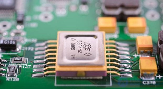
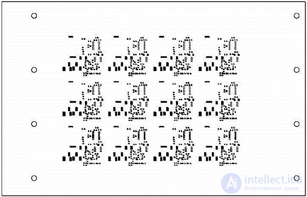
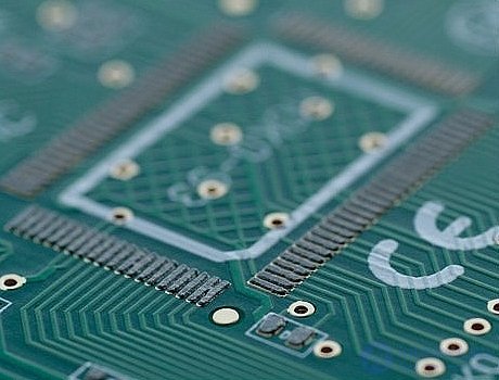
Plot module, made by surface mount technology.
Widespread surface mounting received by the end of the eighties. The novelty consists in using instead of the components on the leads inserted into the holes of the board, the use of components soldered to the pads formed by the conductive pattern. Planar components have no conclusions at all or rarely have short conclusions. The absence of holes for the installation of components reduces the cost of manufacturing the board. Planar components are unified, several times smaller, half the output counterparts. Modules assembled using surface mount technology have a dense arrangement of components, a small distance between components and contact pads. Reducing the length of the conductors improves the transmission of high-frequency and weak signals, decreases unwanted inductance and capacitance. Planar radio elements have a low price. Surface mounting today is much more widespread than mounting into holes. Constantly decreases the cost of assembly.
Surface mounting has several disadvantages. The rigid attachment of the component behind the housing to the conductive pattern leads to the destruction of components exposed to temperature changes. Modules assembled from planar components are afraid of overheating during soldering, bends and shocks. These impacts lead to cracked components. The designer of printed circuit boards must design a conductive pattern that ensures equal speed of heating of the component contacts due to the symmetry of the thermal fields. The technology of group soldering includes the operation mode of the equipment and technological equipment ensuring the same heating rate of the contacts of each component to eliminate scrap. It is required to strictly observe the requirements of transferring the paste to the board and the operation mode of the soldering equipment. Requirements for the transportation and storage of planar components and materials for installation are increasing. Testing the trace of the conductive pattern requires more funds. The cost of technological equipment increases with the release of pilot batches. Repair of modules assembled by surface mounting requires specialized tools.
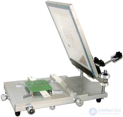
The application of the paste to the contact pads is carried out by the dispenser during the development of the prototype board, and during the serial production of the modules a stencil is used together with the equipment.
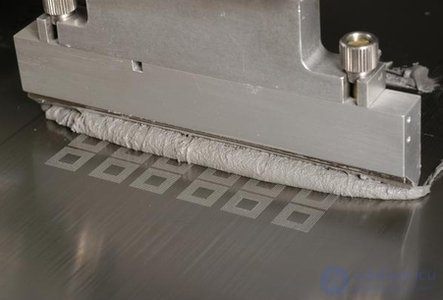
The stencil is made of metal foil having a thickness of from 0.075 to 0.2 mm with holes of a rectangular, trapezoidal or round shape. It can be made of various materials: stainless steel, nickel, bronze. Steel is used more often than other materials for the manufacture of stencils.
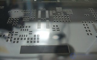
Steel stencil.
To ensure the constancy of the volume of the applied paste and its easy exit to the plate, the holes are made with rounded corners. Metal stencils have a long service life and allow you to quickly and accurately apply solder paste or glue. The stencil, made of stainless steel, has a polished surface, does not require machining, does not stretch. The estimated service life is calculated in tens of thousands of passes. Holes are made by etching, cut out by laser or by electroforming. In the manufacture of laser-cut beam burns hole of the required size with a deviation of not more than 0.005 millimeter. Another advantage of laser cutting is the possibility of changing the taper of the hole walls. Laser cut stencils are highly accurate.
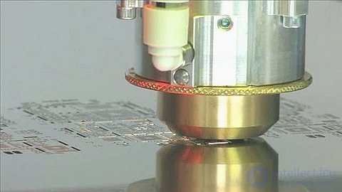
Making a stencil with a laser.
The use of stencils allows the use of boards made of various materials, they are applicable to components with a distance between the terminals of less than 0.6 mm. Making stencils by etching has some drawbacks. The separation of solder paste is difficult due to the incline in the holes, it is possible that the holes are closed, while photolithography makes it difficult to combine patterns on two sides of the stencil blank.
To reduce the production time of modules, several boards are combined into one group board. For a group board, a large stencil is made. Paste is transferred to the group board through one stencil in one pass.
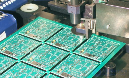
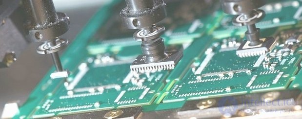
Components are installed on a group board using a machine.
After transferring the paste to the group board, components are installed on it and the paste is melted.
Stencil design is carried out in programs designed for the development of printed circuit boards. Production is made directly according to the file stencil.
Graphic data of the stencil file prepared in the PCAD software development package.
The design of the stencil is conducted, focusing on the conductive pattern of the board and the size of the stencil installation frame. Based on the size of the frame at the disposal of production, it is calculated how many boards to combine into one group.
The stencil is set to frame.
The stencil is fixed between the layers of the frame due to the pins on the bottom layer. The stencil file is filled with holes corresponding to the location of the frame pins. Applying the exact amount of paste reduces the likelihood of conductor closures.
Paste transfer using automatic equipment.
Solder paste is a thick mixture consisting of crushed solder and liquid flux. Example solder alloy: 61% tin, 37% lead, 2% silver. The properties of the paste are dictated by the components of the composition and the size of the solder powder particles. More often, pastes are produced that do not require washing after soldering, or flux residues are washed off with water. Lead-free pastes based on rosin are used much less frequently. The paste should be stored for several months without deterioration of the properties, it should provide a high-quality connection of the components and the board, during melting the solder balls should not form. The paste must hold the components before soldering, not spread when preheated, after the soldering should remain a minimum of flux.
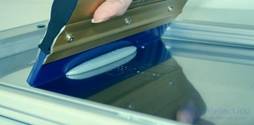
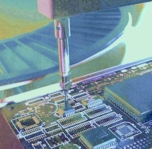
Transfer the paste to the board using a squeegee manually.
Before applying the paste, check that the holes in the stencil match the conductive pattern of the board. Pasta is pressed through the squeegee through the holes. After applying the paste to the board, the stencil is cleaned of the paste residues. As a result, a paste layer remains in the contact pads, located in the center of the contact pad. Squeegees come in various designs and are made from rubber, plastic or metal.

Paste doser controlled by electronic unit.
Manual dispenser is designed for applying solder paste to the contact pads of the board. Instead of using a stencil and related equipment, the paste is applied in small portions in turn to the contact pads using a dispenser. When using a dispenser, more time is spent, but it is not always possible to develop and manufacture a stencil. In conditions of small-scale production and in the manufacture of mock-up samples, it is convenient to use a dispenser. The volume of the paste is determined by the operator or the control unit.
Solder paste is applied to the contact pads of the board.
The installation of planar components on the board with applied paste can be done manually or using automation equipment. With manual installation, inevitable errors in the nominal components. It is impossible to ensure correct and identical clamping of the components to the paste. To eliminate errors in the assembly of modules used varying degrees of automation.
Installing the chip using a semi-automatic.
Semiautomatic installation of components helps the operator to assemble electronic modules. The semiautomatic device moves the container with the required component, a beam of light indicates the point of installation of the component and facilitates assembly in other ways, but the installation of the component is performed by the operator. This reduces the likelihood of rejection during installation. For the price, semi-automatic installers differ up to six times. Their capacity is in the range of 300 ... 1000 components per hour and depends on the operator’s experience.
Installation of components full automatic.
Full automata are used in a stably operating production for the production of large batches of modules. The price of a complete machine is determined by the configuration and functions: supported types of feeders, technical vision, resolution of the installation, the pace of work, the number of heads and others. The price of a complete machine is tens of thousands of dollars.
Contactless soldering . For a reliable connection, soldering should take minimum time with high wetting of the surfaces. This requires active fluxes that do not cause corrosion. The contradiction between performance and reliability can be resolved in the transition to contactless soldering technology. This is due to the need to increase thermal conductivity, which is higher for radiation. The use of contactless soldering technology reduces heating time. Contactless soldering eliminates solder impurities. Damage to components due to static electricity is excluded.
Melting paste can be performed using hot air, infrared radiation, quartz heating, and their combination. Soldering is becoming more common with a laser beam. The temperature of the connections depends on the absorption of heat by the components and the surface of the board. The disadvantage of contactless soldering technology is the dependence of the heating of the soldering area on a variety of factors.
Infrared brazing is performed in special furnaces that can be divided into two classes. Cabinet ovens: the board is stationary in the oven. Conveyor ovens: the board on the conveyor moves through all zones with different temperatures. Inert gas soldering is increasingly used to reduce oxidation.
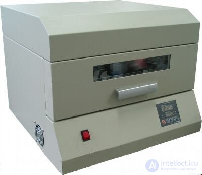
Furnace for melting the solder paste of the cabinet type
infrared radiation with forced air convection.
Furnaces of various designs, mainly of convection type, are intended for infrared soldering. In such furnaces, the board and components are heated by intense infrared radiation, while hot air is simultaneously supplied to the boards and ensures uniform heating. The furnace must withstand the required mode of heating the board. For proper melting of the paste is not enough required temperature. Under the influence of temperature in the paste melting of solder particles occurs, the flux dissolves the oxide film on the surfaces to be joined. A step-by-step heating of the board to the melting point and cooling according to the program recorded in the memory of the furnace controller should occur. This prevents components from thermal shock and board from warping, improves the strength of the connection.
The disadvantage of furnaces is the vibration of the boards under the action of intense air movement. The constant decrease in the dimensions of electronic devices leads to a reduction in the size of the boards. The smaller the board, the more it is subject to movement by the air flow. At the time the paste melts, the components float on the surface of the melted solder and a slight vibration of the board is enough to dislodge the component or fall out of the board. The air flow inside the furnace moves with different intensity. In the manufacture of the lot, the entire lattice is occupied by the boards and from loading to loading the board in the same area of the furnace vibrates and loses components. It is impossible to make a snap for fixing the boards. It is impossible to use metal in the conditions of infrared radiation - overheating of the boards at fixing points is inevitable. Requires pottery. Making ceramic tooling for each type of boards is expensive.
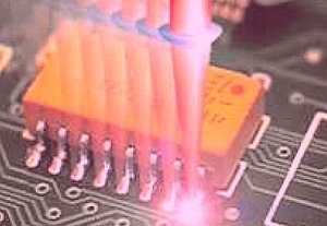
Soldering using a laser beam is the most promising of all soldering technologies. The first industrial unit was created in the United States in 1976 using a gas laser, and in 1982 using a solid-state laser. Today, laser soldering, more than other technologies, is close to perfect soldering. Due to the concentration of power by a laser beam in a region with a diameter of about 0.1 mm, it became possible to solder components that are sensitive to heat and eliminate distortion of the boards. The method is suitable for modules with a dense arrangement of components, which have a small distance between the terminals. At installation circuit and solder balls are not formed. The absence of inertia of radiation exposure allows heating with pulses of short duration of 1 ... 10 ms and accurate metering of energy. There is a high stability of temperature-time regimes. The time of continuous soldering is 0.3 ... 0.8 s, the temperature is 220 ... 250 ° C. The time of the laser pulse soldering is 0.02 ... 0.08 s, the temperature is 250 ... 300 ° C. By changing the energy of the laser beam transmitted to the soldering area, it is possible to change the temperature over a wide range. Cooling with pulse brazing is faster than with continuous brazing. Short-term exposure to a laser beam reduces oxidation. Preheating of the board is not required, which is a big advantage in comparison with wave soldering. The solder melts quickly, wets the surfaces and fills the gap, cools quickly, which contributes to a good connection. No special gas environment required. Heat-resistant adhesives are not required for double-sided installation. Soldering have a glossy surface and are of high quality. The technology of laser soldering allows you to create complete machines. It becomes possible to carry out selective soldering, in which individual components are installed later. Installation capacity can up to 2000 rations per hour.
The disadvantage that restrains the spread of laser soldering is the price of the equipment. Also inhibited is the proliferation of the need for new fluxes and how to dose them.
Laser radiation enables precision soldering of planar components. For soldering planar components used laser diodes and light guides.
Research is underway to improve laser soldering. The possibilities of this technology are far from being exhausted, and there is reason to expect acquaintance with new faces of laser soldering. Known to increase the activity of surfaces with a pulsed laser exposure. No-flux soldering is being developed using modulated laser radiation. A performance increase is possible with a split beam or as a result of applying methods to direct radiation to all connections belonging to a single chip or to the entire board. There are prospects for the use of laser soldering with mixed installation.
Bilateral surface mounting can be done in various ways. The problem is that if you put the paste on both sides, put the components and melt the paste, then you can not do it. Components on the underside will fall off. Therefore, at first, paste and glue are applied on one side of the board and the components are installed. Then the paste is melted and the glue is polymerized. The board is turned over, the paste is applied and the components are installed on the second side of the board, after which the paste is again heated and melted on the second side.

Comments
To leave a comment
Design and engineering of electronic equipment
Terms: Design and engineering of electronic equipment