Lecture
The method was invented by the Institute of Spectroscopy RAS.
Images are drawn using an atomic pinhole camera with a mask of tiny holes through which a beam of atoms penetrates.
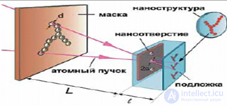
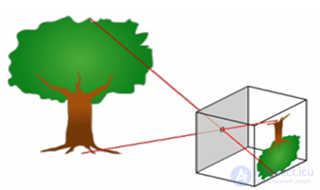
The idea is the development of the long-known idea of a pinhole camera, which allows you to create optical images using a small hole in the screen.
An object located at a certain distance from the screen creates its image in a darkened chamber due to the presence of a small hole in the wall of the chamber. The image is formed on the rear wall of the camera without the use of any additional optics like the usual glass lenses. Resolution is determined by the size of the hole and the distance between the hole and the back wall.
If you use a beam of neutral atoms instead of light, you can create an image of a mask pattern, which is formed by the condensation of neutral atoms on the surface.
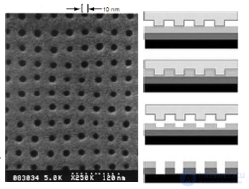
An image of nanometer sizes is formed if the hole size lies in the nanometer range, and the distance between the hole and the surface is in the micrometer range.
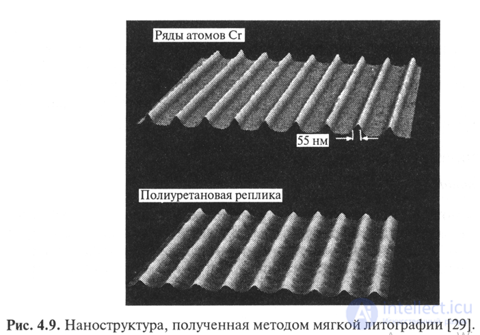
The left side of the figure shows the nanoholes in the membrane. On the right are the obtained nanostructures.
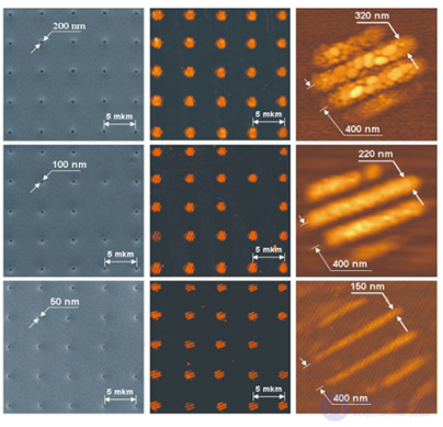
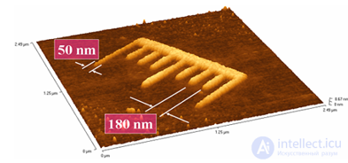
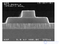
Below is an example of the resulting structure
Modern lithography is becoming more and more expensive as it improves and develops.
Alternative lithographic methods are being developed.
Imprint lithography
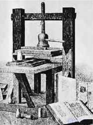
The oldest type of lithography
A family of new micro- and nanolithographic methods has been implemented.
Nanoimprint lithography (NIL)
Thermal nanoimprint lithography
Photonanoimprint lithography
Soft lithography
Nanoimprint lithography allows obtaining a resolution of ~ 10 nm
Since the 1990s, nanoimprint lithography (NRL) has arisen and developed as one of the most universal methods for the formation of nanoscale structures, the sizes of which lie in the range from 10 nm to units of microns.
Today, NIL is one of the technologies that chip designers rely on.
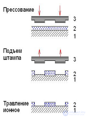
Three main components are required for the implementation of LLL on a substrate: a stamp with the corresponding parts, the material on which the fingerprint is made (which is usually used as a polymer resist), printing equipment with appropriate control of temperature, pressure and relative position of the stamp and the substrate.
Nanoimprint Lithography (NanoImprint Lithography - NIL) and its variations are based on the principle of mechanical modification of a polymer film using a stamper (nanomask), followed by thermomechanical processing (hot stamping) or ultraviolet treatment.
The resulting film can be used as directly the final structure, and for subsequent steps as a nanoscale, for explosive lithography (lift-off), as a template for the formation of 3D structures.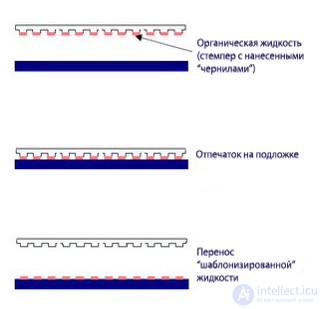
In the process of thermal imprinting, the stamp is pressed under high pressure and at high temperature into the polymer layer, which is currently in the liquid state. When cooling, the polymer fixes the desired shape, after which the stamp is removed.
• Thermal nanoimprint lithography
–– A thermoplastic polymer is applied to the surface of the substrate
–A mold with the desired relief on the surface is pressed into the polymer when heated to a polymer transition temperature
–After cooling, the mold is removed
–– Etching of the obtained structure to transfer the structure to the substrate
–– The same method with laser heating
• Photonanoimprint lithography
–Using photoresist
–The form is made transparent
–When pressed, a UV light is applied to cure the resist
Electrochemical nanomiprint lithography
Electrochemical transfer of metal to a substrate
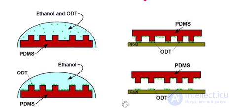
Soft (Soft) lithography - microcontact printing according to the following steps:
- A mold is made from an elastomeric material (for example, polydimethylsiloxane PDMS) according to the template
- Apply a monolayer of "ink" on the form (for example, octadecantiol ODT in ethanol solution)
- ODT is deposited on the mold (self-assembly)
- The shape is pressed to the substrate (with a sprayed thin layer of gold)
- The pattern is transferred to the substrate by etching.
Differences nanoimprint lithography
Advantages
disadvantages
Nanoprint lithography is intended for transferring an image of a nanostructure or an electronic circuit onto a coated substrate and including deformation of the coating by a stamp followed by etching of the deformed coating and the formation of a nanostructure or electronic circuit elements on the substrate.
In the method of nano-printing lithography, the image is formed mainly due to the physical deformation of the resist by the mold (stamp), and not due to the modification of the chemical structure of the resist by irradiation, as in conventional lithography.
This fundamental difference relieves the NPL from many problems associated with standard lithography methods (diffusion limit, scattering, and chemical processes).
As a result, using NPLs, it is possible to obtain structures with a size of less than 10 nm over large areas at an inexpensive and high yield, which is not available for all existing lithography methods.
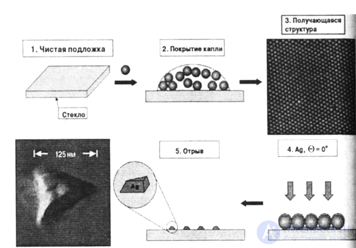
Литография наносферами

Comments
To leave a comment
Design and engineering of electronic equipment
Terms: Design and engineering of electronic equipment