Lecture
The printed circuit board is a plate with holes, made of an insulator, on which are conductors with contact pads for installation by soldering electronic components. The transition from bulk installation to mounting on printed circuit boards has become a new stage in the production of electronics. Installation in volume was replaced by installation on the plane. Assembling an appliance with the use of surround installation technology is harder than using board mounting. Performing surround installation requires attaching wires to protect against vibration, the components are installed in special media. The signal branching along several wires is performed using terminals, which, together with the component holders, are mounted on the chassis of the instrument housing. Development of the device based on the technology of volumetric installation requires from the designer a long study of mechanical fastenings of the circuit elements.
The board combines the functions of the conductor carrier and the component carrier. With the introduction of electronics into the production of boards, the possibility of automation of installation appeared. Significantly simplified repair and configuration. A significant reduction in the share of volumetric installation in the assembly of an electronic device has reduced costs and reduced the number of errors. If earlier for assembly of the electric circuit a large number of wires was required, now one or several boards are enough. The location of the conductors is identical when replicating the boards, which makes it possible to produce devices with high repeatability of parameters due to the capacitance and inductance between the electrical connections and their electrical resistance. Troubleshooting can be done by replacing the boards installed in the connector instead of checking the set of wires that were used for surround installation. The use of boards reduces metal consumption, size and weight, allows the use of microcircuits, improves heat removal, which improves the characteristics of devices and reduces the cost compared to the use of volumetric mounting.
The advantages of mounting on boards over bulk installation made boards the main choice of electronics manufacturers. The need for a large number of boards constantly stimulates the improvement of the production of printed circuit boards and the emergence of new technologies and materials in this area. With the advent of PCB technology, the development of electronics has been simplified.
The main elements of the PCB design are dielectric base and conductive pattern placed on one or two sides. Multi-layer boards are becoming increasingly common. To solve some engineering problems, boards are made that are made on a flexible basis. Sometimes it is appropriate to use a combination of two or more materials in the construction of a single board and a combination of flexible and solid bases.
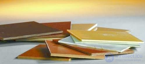
Different materials of the base boards.
Steklotekstolit more often than other materials used for the manufacture of the base rigid board. Fiberglass has good dielectric properties, mechanical strength and chemical resistance, durability and safety, it is allowed to operate fiberglass in conditions of high humidity. The most important characteristics of the material are the electrically insulating properties and the second most important characteristic is the glass transition temperature Tg, which limits the scope. The transition temperature of the material from the solid to the plastic state is the glass transition temperature. The higher the glass transition temperature of the resin, the lower the linear expansion coefficient of the dielectric, leading to the destruction of the board conductors. The value of the glass transition temperature depends on the molecular weight of the resin molecules used in the manufacture of the material. The appearance and increase of elasticity occurs in a certain range of temperatures. The central value within this range is called the glass transition temperature. The increase in glass transition temperature is possible with the improvement of the production technology of fiberglass.
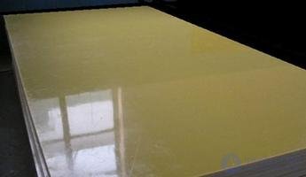
Steklotekstolit sheets.
Glass fiber is a material produced by hot pressing of several layers of glass fabric impregnated with a binder composition - epoxy or phenol-formaldehyde resin. There are many brands produced for various operating conditions. Developed various requirements for manufacturing technology. The flash point of various grades of fiberglass from 300 to 500 ° C. STEF is a common domestic brand of fiberglass laminate, which stands for epoxy-phenolic glass fiber textolite. STEF-1 differs from STEF only in its manufacturing technology, which makes it more suitable for machining. STEF-U has improved mechanical and electrically insulating properties in comparison with the STEF-1 brand.
Some characteristics of fiberglass grades.
|
|
STEF |
STEF-1 |
STEF-U |
STEF-T |
CTT |
ST-ETF |
|
Heat resistance class ° C |
155 |
180 |
||||
|
Colour |
Yellow |
brown |
||||
A variation of this material is foil fiberglass laminate used in the manufacture of boards.
Foil material refers to a base material of a board that has a conductive foil on one or both sides — sheet conductor material intended to form a conductive board pattern. The success of the production of boards and the reliability of the manufactured device depend on the quality and parameters of the material used.
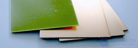
Unilateral foiled fiberglass.
Foil fiberglass has many brands. For the production of boards used domestic brands in accordance with GOST produced by our manufacturers: SF, SONF-U, STF, STNF, SNF, DFM-59, SFVN and brands of imported glass fiber FR-4, FR-5, CEM-3 with many modifications. For the manufacture of boards designed to work in conditions of normal and high humidity at temperatures from -60 to +85 ° C, the SF brand is used, which has many types, one of which is SF-1-35G.
Designations in the name of SF-1-35G.
|
Symbol |
Decryption |
|
SF |
fiberglass foil |
|
one |
unilateral |
|
35 |
35 micron foil thickness |
|
R |
galvanically resistant foil |
For the production of most electronic devices, the SONF-U brand can be used, its operating temperature is from -60 to +155 ° С. Designations in the name: C and F - foil-laminated glass fiber, HE is of general purpose, Y - contains bromine-containing additive and belongs to the class of non-combustible plastics. The thickness of the foil placed on the base has values from a range of 18, 35, 50, 70, 105 microns. The thickness of the foiled fiberglass is in the range from 0.5 to 3 mm.

Foiled glass fiber laminate.
Parameters of some brands of foil fiberglass.
|
Mark |
Limit operating temperature ° C to |
Glass transition temperature Tg ° C |
|
SF-1-35G, SF-2-35G, SF-1-50G, SF-2-50G, SF-1N-50G, SF-2N-50G, SF-1-70G, SF-2-70G |
85 |
|
|
SFN |
100 |
|
|
STF-1-35G, STF-2-35G |
105 |
|
|
STNF |
110 |
|
|
SONF-U |
155 |
|
|
CEM-3 |
|
130 |
|
FR-4 |
|
135-170 |
|
FR-5 |
|
160 |
|
DFM-59 |
|
270 |
|
SPWN |
|
290 |
FR-4 fireproof (Fire Retardent) imported foil glass fiber. FR-4 today the most common brand of material for the production of printed circuit boards. High technological and operational characteristics determined the popularity of this material.
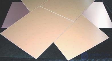
Unilateral foiled fiberglass laminate CEM-3.
CEM-3 is an imported material (Composite Epoxy Material) that most closely matches the FR-4 foil-clad fiberglass, at a price of 10-15% less. It is a glass fiber base between the two outer layers of fiberglass. Suitable for plating holes. CEM-3 milky white or transparent material, very smooth. The material is easily drilled and stamped. In addition to foil PCB for the manufacture of boards used a variety of different materials.

Unilateral foil getinaks.
Foil getinaks are designed for the manufacture of boards intended for operation at normal air humidity with one- or two-sided mounting of parts without metallization of holes. The technological difference between Getinax and fiberglass consists in using paper, rather than glass fiber, in its production. The material is cheap and easily stampable. It has good electrical characteristics in normal conditions. The material has disadvantages: poor chemical resistance and poor heat resistance, hygroscopicity.
Parameters of some brands of foil getinaks.
|
Mark |
Operating temperature not more than ° С |
Glass transition temperature Tg ° C |
|
GF-1-35, GF-1-35G, GF-2-35, GF-2-35G, GF-1-50, GF-1-50G, GF-2-50, GF-2-50G |
85 |
|
|
FR-2 |
|
105 |
|
FR-3 |
|
110 |
|
FR-1 |
|
130 |
|
CEM-1 |
|
130 |
Domestic foiled Getinaks of the GF-1-35, GF-2-35, GF-1-50 and GF-2-50 grades are designed for operation at a relative humidity of 45 - 76% and a temperature of 15 - 35 С °, the base material has a brown color . XPC, FR-1, FR-2 - imported foil getinaks. These materials have a base of paper with a phenolic filler, the materials are well stamped.
FR-3 is a modification of FR-2, but epoxy resin is used as a filler instead of phenolic resin. The material is intended for the production of boards without plating holes.
CEM-1 - a material consisting of epoxy resin (Composite Epoxy Material) on a paper base with a single layer of fiberglass. Designed for the production of boards without metallization of holes, the material is well stamped. Usually milky white or milky yellow.
Other foiled materials are used for more stringent operating conditions, but have a higher price. Their base is made on the basis of chemical compounds that improve the properties of the boards: ceramics, aramid, polyester, polyimide resin, bismaleimide-triazine, cyanate ester, fluoroplast.
Parameters of some brands of foil materials.
|
Mark |
Glass transition temperature Tg ° C |
|
BT |
180-220 |
|
CE |
230 |
|
PD |
260 |
|
PTFE |
240-280 |
|
CHn |
300 |
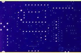
The term PCR (rrinting plate) appeared due to the use of printing technology in the production of boards. In translation, the rrinting plate means a printing form or matrix. The conductive pattern on the board is formed by removing unnecessary foil fragments using a single photomask for a batch of boards. At the first stage of manufacturing in the board blank, holes are drilled for mounting components and vias to ensure electrical contact between conductors located in different layers.
The transition hole on the board without applying a protective mask.
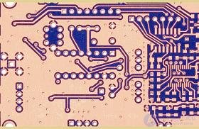
After drilling holes are prepared for the deposition of metal by chemical cleaning. Mounting and vias are metallized by deposition of several layers of metal on the surface of the walls. Metallized holes must withstand at least 4 (multilayer at least 3) repacks.
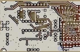
If the board is designed to use one-sided foil material and has one layer of conductive pattern, then there are no vias, the board’s reliability increases, and the price decreases.

Board preparation area with plated holes.
A photosensitive substance is applied to the foiled surface.
Plot the board with a layer of photosensitive substance.
The electronic file made by the developer of the printed circuit board, contains the location of the holes and a conductive pattern. The file is converted to a photo mask. The board is illuminated through the photomask pattern printed circuit board. The manifestation of the photosensitive layer.
Plot the board with a developed photosensitive layer.
After development, some areas of the photosensitive layer are washed away, others do not dissolve and remain on the foil, forming a pattern of conductors, contact pads and signs.

Plot the workpiece after the removal of excess light-sensitive substances.
Then the board is immersed in a chemical solution that reacts with copper. The developed photosensitive substance protects the copper foil from the effects of the etching solution. Copper foil exposed areas are etched in chemical solution.
Plot site after etching.
Photosensitive substance is washed off. A protective mask is applied to the board to protect against short-circuits during installation and the influence of external factors on the conductors and base of the board.
Plot board with a protective mask.
Optionally, the board can be marked: the reference designations of the circuit elements, the decimal number of the board’s development, the names of the solder pins and others.
The plot of the board with inscriptions.
On the board, protected by a mask, the soldering areas are covered with solder. Most manufacturers exclude lead in their products. Immersion tin is increasingly used - a chemical coating that provides high quality printed circuit boards. The coating provides good soldering during storage of the board for several years and is compatible with all types of soldering, allowing for several repackings. If necessary, selective gilding and nickel plating is performed.
Board area with tin-plated contacts.
At the final stages of production, mounting holes are drilled in the board, which are used to mechanically fasten the board to the chassis or to mechanically fasten the elements to the printed circuit board. At the end of production, the board is milled around the contour, giving the exact dimensions set by the developer.
Production of boards with more than two conductive layers is more difficult. They look like a layer cake consisting of thin double-sided boards and interlayers of resin-impregnated fiberglass. The layer is called prepreg, its thickness is 180-100 microns. Multilayer boards can have openings for interlayer connections only between the layers and not passing through the board. The transition hole for the connection of the outer layer and the inner one is blind, between the inner layers is hidden. Boards with blind holes have a higher price.
After control, the fee is sent to the warehouse. The capabilities of board manufacturers are dictated by a set of mastered technologies; therefore, before placing an order for the production of a board, you should consult with the manufacturer.

Comments
To leave a comment
Design and engineering of electronic equipment
Terms: Design and engineering of electronic equipment