Lecture
General Provisions
The sizes of elements in the photolithographic process are fundamentally limited by the wavelength of the radiation used. To further reduce the elements of IP, it is necessary to use electron beam and X-ray lithography.
The use of electron beam lithography allows you to:
a) receive picture elements with sizes less than or equal to 0.01 μm (for photolithography at least 0.5 μm);
b) with high accuracy to control the dose of the electron beam incident on the resist and the substrate;
c) it is easy to deflect and modulate the electron beam with high accuracy by electric and magnetic fields;
d) in some cases form the topology of the circuit directly on the plate;
d) automate the technology of creating a topological drawing;
f) profile the electron beam.
A significant drawback of electron beam lithography is its low productivity compared to optical.
Creating a submicron topology requires focusing the electron beam into a spot with a diameter of about 0.01 microns. With such linear dimensions of the topology elements, scanning and interruption of the electron beam can only be carried out using a computer. The control system at the same time operates at frequencies of several megahertz.
Electron lithography or electron beam lithography is an electron beam lithography method.
Electron beam lithography is a method of manufacturing submicron and nanoscale topological elements by exposure of electrically sensitive surfaces by an electron beam.
The method is similar to photolithography, but uses electrons instead of photons. Since the electron wavelength is much shorter than that of a photon, diffraction does not limit resolution.
The electron beam scans the surface of the electron resist, repeating the pattern embedded in the control computer, and allowing to achieve a resolution of 1 nm due to the shorter electron wavelength compared to light.
Electronic lithography is used to create mask patterns for photolithography, in the production of piece components where nanometer resolution is required, in industry and in scientific activity.
Electronic resistors, interaction of electrons with resist and substrate material
The resistors used in electron beam lithography have the same requirements as photoresists in photolithography. In electronic resistors, chain splitting processes in polymer molecules usually occur under the influence of ionizing radiation (electron beam). In this case, the molecular weight of the polymer decreases and it becomes soluble in a special solvent that does not act on high molecular weight material. Such polymers are called positive electronic resistors. In negative electron resistors under the influence of electron irradiation, the processes of formation of cross-links in the polymer molecules and the formation of a complex three-dimensional structure occur. Non-irradiated sections of the polymer in this case have a significantly lower molecular weight compared to the irradiated ones and are removed by dissolution. When an electron beam penetrates the resist and the substrate, the electrons interact with the substance, their elastic and inelastic scattering (Fig. 2).
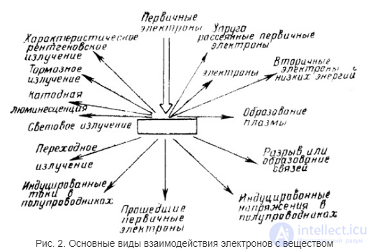
Thus, the exposure dose of one section of the plate affects the exposure of neighboring areas, which leads to blurring the profile of the distribution of exposure energy. This phenomenon in electron beam lithography is called the proximity effect.
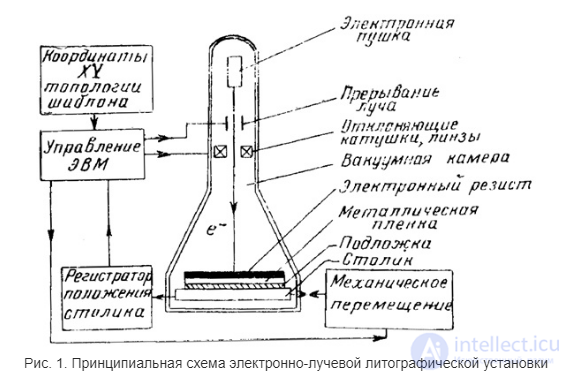
Installation diagram for electronic lithography
The installation scheme is extremely simple, easily scalable and does not require additional modules (vacuum system, high-voltage power supply, etc.).
A thin film of silicon nitride can attenuate the flow of β-electrons to acceptable energy values, and a tungsten mask effectively absorbs electrons in those places where it is required.
It is also worth noting that this system allows you to immediately illuminate large areas of substrates with a photoresist, significantly accelerating this procedure
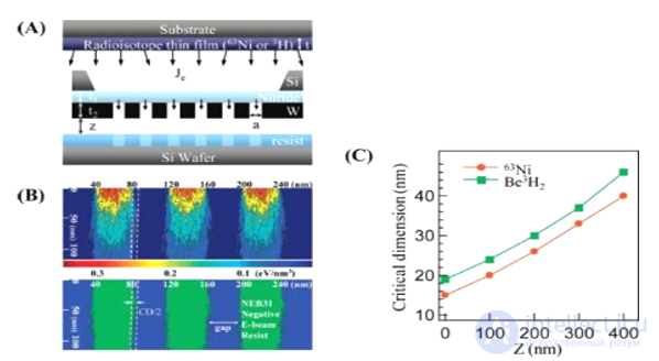
(A) Installation diagram for SPEL.
(B) 3D modeling of electron behavior using the Monte Carlo method.
(C) Dependence of obtained permission on Z
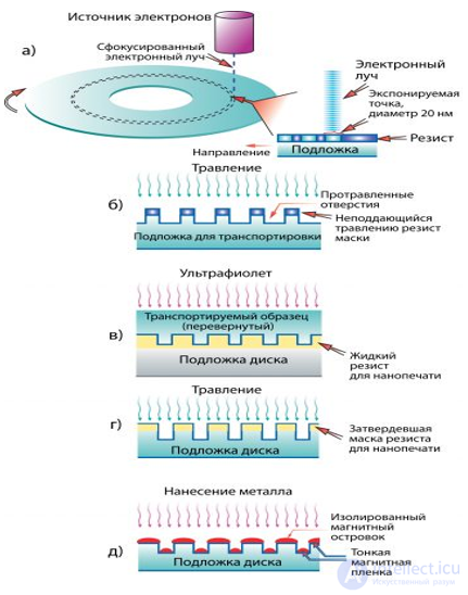
Direct recording electronic lithography, no photo mask
Used for the manufacture of photomasks for photolithography
Scanning an electron beam over a photoresist layer
A resolution of several nm can be achieved.
Very long process
Not applicable in mass production conditions.
The ability to quickly make prototypes without making masks
It is possible to correct single defects of masks and lithography using an electron beam
Equipment
Almost any scanning electron microscope
Special optimized installation
Similarly, ion beam lithography works.
• Electronic lithography systems for commercial use are very expensive (> $ 4 million). For scientific research, they usually use an electron microscope converted into an electronic lithography system using relatively cheap accessories (<$ 100 thousand). Such converted systems have created a line width of ~ 20 nm since the 1990s, while specialized equipment will allow a resolution of less than 10 nm up to 1 nm.
• Electron beam lithography systems can be classified according to the shape of the beam and according to the beam deflection strategy.
Older systems used Gaussian beams and scanning was performed using the raster method. Newer systems use both Gaussian beams and a shaped beam shape that can be deflected to various positions in the recording field (this is also called vector scanning).

Comments
To leave a comment
Design and engineering of electronic equipment
Terms: Design and engineering of electronic equipment