Lecture
Optical nanolithography uses various optical methods.
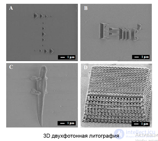
Two-photon lithography
Two-photon polymerization processes allow reaching a resolution of ~ 200 nm
The probability of a reaction depends on the intensity of the fourth degree
3D lithography possible
Near Field Lithography
Photochemical or photophysical exposure using the near field of the probe
Near Field Phase Lithography
Plasmon Seal
Light amplification using plasmon resonance on metal nanoparticles near the surface
Laser interference lithography (LIL) is a production method using high-intensity lasers, a method for recording large-area structures with a resolution much higher than 5 nm without using a resist.
Laser interference nanolithography uses 2 lasers. The first of them - generates continuous radiation with a wavelength of 1064 microns and is a trap beam.
This radiation passes through the axicon lens and forms into a beam of a Bessel shape, which is then split into four parallel beams using two Mach-Zander interferometers.
The power of each of the Bessel beams is of the order of 150 mW and is used to capture a single spherical lens with a diameter of 0.76 μm.
The working laser generates pulsed radiation at a wavelength of 355 nm; the pulse length is of the order of 15 ns, the energy of each of the pulses is within 150 nJ - 8 μJ.
The beam passes through the microspheres and falls on the substrate.
Image recording is performed by moving the substrate relative to the optical traps.
3D двухфотонная литография

Comments
To leave a comment
Design and engineering of electronic equipment
Terms: Design and engineering of electronic equipment