Lecture
The printed circuit board (English printed circuit board, PCB , or printed wiring board, PWB ) is a dielectric plate, on the surface and / or in the volume of which electrically conductive electronic circuits are formed. The printed circuit board is designed for the electrical and mechanical connection of various electronic components. The electronic components on the printed circuit board are connected by their leads to the elements of the conductive pattern, usually by soldering.
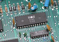
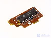

In contrast to mounted installation, on a printed circuit board, the electrically conductive pattern is made of foil, which is entirely located on a solid insulating base. The printed circuit board contains mounting holes and contact pads for mounting of pin or planar components. In addition, in the printed circuit boards there are vias for the electrical connection of the foil sections located on different layers of the board. From the external sides, a protective coating (“solder mask”) and marking (auxiliary drawing and text according to the design documentation) are usually applied to the board.
Depending on the number of layers with a conductive pattern, printed circuit boards are divided into:
As the complexity of the designed devices and installation density increases, the number of layers on the boards increases [1] .
According to the properties of the base material :
Printed circuit boards may have their own characteristics, due to their purpose and requirements for special operating conditions (for example, an extended temperature range ) or application features (for example, boards for devices operating at high frequencies ).
The basis of the printed circuit board is a dielectric, the most commonly used materials such as glass fiber, getinaks.
Also, the basis of printed circuit boards can serve as a metal base coated with a dielectric (for example, anodized aluminum), a copper foil of tracks is applied over the dielectric. Such printed circuit boards are used in power electronics for efficient heat removal from electronic components. In this case, the metal base plate is attached to the radiator.
As a material for printed circuit boards operating in the microwave range and at temperatures up to 260 ° C, fiberglass-reinforced fluoroplastic (for example, FAF-4D) [2] and ceramics are used.
Flexible boards are made from polyimide materials such as Kapton.
The design of boards takes place in specialized computer-aided design programs. The most famous are P-CAD, OrCAD, TopoR, Altium Designer, Specctra, Proteus, gEDA, KiCad, etc. [3] The design process itself is often referred to as the slang word wiring , implying the process of wiring.
In Russia, there are standards for the design documentation of printed circuit boards in the framework of the Unified system for design documentation:
Other standards for printed circuit boards:
Consider the typical process of developing a board from a ready-made circuit diagram: [4]
Printed circuit board manufacturers often encounter non-obvious design errors by novice engineers. [6] The most common mistakes:
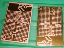
The production of PP is possible additive or subtractive method. In the additive method, the conductive pattern is formed on a non-foiled material by chemical copper plating through a protective mask previously applied to the material. In the subtractive method, the conductive pattern is formed on the foiled material by removing unnecessary foil areas. In modern industry, only the subtractive method is used.
The whole process of manufacturing printed circuit boards can be divided into four stages:
Often under the manufacture of printed circuit boards understand only the processing of the workpiece (foil material). A typical process for treating foiled material consists of several stages: drilling of vias, obtaining a pattern of conductors by removing excess copper foil, plating holes, applying protective coatings and tinning, marking. [7] For multilayer printed circuit boards, extrusion of the final board from several blanks is added.
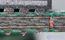
Foil material is a flat dielectric sheet with copper foil glued to it. As a rule, fiberglass laminate is used as a dielectric. In the old or very cheap equipment, textolite is used on a fabric or paper base, sometimes referred to as getinax. Fluorine-containing polymers (fluoroplastics) are used in microwave devices. The thickness of the dielectric is determined by the required mechanical and electrical strength, the most widespread thickness is 1.5 mm.
A dielectric sheet of copper foil is glued to the dielectric on one or two sides. The foil thickness is determined by the currents under which the board is designed. The most widespread foil is 18 and 35 microns thick, 70, 105 and 140 microns are much less common. Such values are based on standard copper thicknesses in imported materials, in which the thickness of a layer of copper foil is calculated in ounces (oz) per square foot. 18 microns corresponds to ½ oz and 35 microns - 1 oz.
A separate group of materials consists of aluminum metal printed circuit boards. [8] They can be divided into two groups.
The first group consists of solutions in the form of an aluminum sheet with a high-quality oxidized surface on which copper foil is glued. Such boards cannot be drilled; therefore, they are usually only made one-sided. The processing of such foiled materials is carried out according to traditional technologies of chemical drawing of the image. Sometimes copper or steel laminated with a thin insulator and foil is used instead of aluminum. Copper has a higher thermal conductivity, stainless steel board provides corrosion resistance. [9]
The second group involves the creation of a conductive pattern directly in the aluminum base. For this purpose, aluminum sheet is oxidized not only on the surface, but also to the entire depth of the substrate, according to the pattern of conductive areas given by the photomask. [ten]
In the manufacture of boards used chemical, electrolytic or mechanical methods of reproducing the desired conductive pattern, as well as their combinations.
The chemical method of manufacturing printed circuit boards from the finished foil material consists of two main stages: applying a protective layer on the foil and etching unprotected areas by chemical methods.
In industry, the protective layer is applied by photolithography using an ultraviolet-sensitive photoresist, photomask and an ultraviolet light source. Copper foil is completely covered with photoresist, after which the pattern of the tracks from the photomask is transferred to the photoresist by flare. The illuminated photoresist is washed away, exposing the copper foil for pickling, the non-illuminated photoresist is fixed on the foil, protecting it from etching.
The photoresist is liquid or film. Liquid photoresist is applied in an industrial environment, as it is sensitive to non-compliance with the application technology. Film photoresist is popular for the manual manufacture of boards, but it is more expensive. The photomask is a UV-transparent material with a printed pattern of tracks on it. After exposure, the photoresist appears and is fixed as in the usual photochemical process.
In amateur conditions, a protective layer in the form of a lacquer or paint can be applied by silk-screen or manually. Radio amateurs apply toner transfer from an image printed on a laser printer (“laser-iron technology”) to form an etching mask on a foil.
Under the etching of the foil understand the chemical process of transferring copper into soluble compounds. Unprotected foil is etched, most often, in a solution of ferric chloride or in a solution of other chemicals, such as copper sulfate, ammonium persulfate, ammonium copper chloride, ammonium copper sulfate, based on chloroforite, based on chromic anhydride [11] . When using ferric chloride, the board etching process goes as follows: FeCl 3 + Cu → FeCl 2 + CuCl. Typical concentration of the solution is 400 g / l, temperature up to 35 ° C. When ammonium persulfate is used, the board etching process is as follows: (NH 4 ) 2 S 2 O 8 + Cu → (NH 4 ) 2 SO 4 + CuSO 4 [11] .
After etching, the protective foil pattern is washed off.
Mechanical manufacturing method involves the use of milling and engraving machines or other tools for the mechanical removal of the foil layer from specified areas.
Until recently, laser engraving of printed circuit boards was poorly distributed due to the good reflective properties of copper at the wavelength of the most common high-power gas CO lasers. In connection with the progress in the field of laser construction, industrial prototyping systems based on lasers have begun to appear. [12]
Transition and mounting holes can be drilled, pierced mechanically (in soft materials like getinaks) or by laser (very thin vias). Hole metallization is usually carried out chemically or mechanically.
Mechanical plating of the holes is carried out with special rivets, soldered with wires or by pouring the hole with conductive glue. The mechanical method is expensive in production and therefore is used extremely rarely, usually in highly reliable piece solutions, special high-current equipment or amateur radio conditions.
When chemical metallization in foil blanks, the holes are first drilled, then they are metallized and only then the foil is etched to obtain a print pattern. Chemical metallization of holes is a multistage complex process, sensitive to the quality of reagents and compliance with technology. Therefore, in amateur radio conditions almost never used. Simplified consists of the following stages:
Многослойные платы (с числом слоев металлизации более 2) собираются из стопки тонких двух- или однослойных печатных плат, изготовленных традиционным способом (кроме наружных слоев пакета — их пока оставляют с нетронутой фольгой). Их собирают «бутербродом» со специальными прокладками (препреги). Далее выполняется прессование в печи, сверление и металлизация переходных отверстий. В последнюю очередь делают травление фольги внешних слоев. [one]
Переходные отверстия в таких платах могут также делаться до прессования. Если отверстия делаются до прессования, то можно получать платы с так называемыми глухими отверстиями (когда отверстие есть только в одном слое бутерброда), что позволяет уплотнить компоновку.
Возможны такие покрытия как:
На одном листе заготовки зачастую помещается множество отдельных плат. Весь процесс обработки фольгированной заготовки они проходят как одна плата, и только в конце их готовят к разделению. Если платы прямоугольные, то фрезеруют несквозные канавки, облегчающие последующее разламывание плат (скрайбирование, отангл. scribe царапать). Если платы сложной формы, то делают сквозную фрезеровку, оставляя узкие мостики, чтобы платы не рассыпались. Для плат без металлизации вместо фрезеровки иногда сверлят ряд отверстий с маленьким шагом. Сверление крепежных (неметаллизированных) отверстий также происходит на этом этапе.
См. : ГОСТ 23665-79 Платы печатные. Обработка контура. Требования к типовым технологическим процессам.
По типовому техпроцессу отделение плат от заготовки происходит уже после монтажа компонентов.
Пайка является основным методом монтажа компонентов на печатные платы. Пайка может выполняться как вручную паяльником, так и с помощью специально разработанных специфических технологий.
Основной метод автоматизированной групповой пайки для выводных компонентов. С помощью механических активаторов создается длинная волна расплавленного припоя. Плату проводят над волной так, чтобы волна едва коснулась нижней поверхности платы. При этом выводы заранее установленных выводных компонентов смачиваются волной и припаиваются к плате. Флюс наносится на плату губчатым штемпелем.
Основной метод групповой пайки планарных компонентов. На контактные площадки печатной платы через трафарет наносится специальная паяльная паста (порошок припоя в пастообразном флюсе). Затем устанавливаются планарные компоненты. Затем плату с установленными компонентами подают в специальную печь, где флюс паяльной пасты активизируется, а порошок припоя плавится, припаивая компонент.
Если такой монтаж компонентов выполняется с двух сторон, то плата подвергается этой процедуре дважды — отдельно для каждой стороны монтажа. Тяжелые планарные компоненты устанавливаются на капельки клея, которые не позволяют им упасть с перевернутой платы во время второй пайки. Легкие компоненты удерживаются на плате за счет поверхностного натяжения припоя.
После пайки плату обрабатывают растворителями с целью удаления остатков флюса и других загрязнений, либо, при использовании безотмывочной паяльной пасты, плата готова сразу для некоторых условий эксплуатации.
Установка компонентов может выполняться как вручную, так и на специальных автоматах-установщиках. Автоматическая установка уменьшает вероятность ошибки и значительно ускоряет процесс (лучшие автоматы устанавливают несколько компонентов в секунду).
После пайки печатную плату с компонентами покрывают защитными составами: гидрофобизаторами, лаками, средствами защиты открытых контактов.
Для массового промышленного производства печатных плат разработаны автоматизированные методики контроля качества. Для контроля качества обработки заготовки применяются электрические тесты на целостность проводников и отсутствие замыканий. При контроле качества монтажа электронных компонентов применяют оптические методы контроля .
Оптический контроль качества монтажа выполняется с помощью специализированных стендов с видеокамерами высокого разрешения. Стенды встраиваются в технологическую линию на этапах:
Подложки гибридных микросхем представляют собой нечто похожее на керамическую печатную плату, однако обычно используют другие техпроцессы:
Керамические корпуса электронных микросхем и некоторых других компонентов также выполняются с привлечением технологий гибридных микросхем.
Мембранные клавиатуры часто выполняют на пленках методом шелкографии и спекания легкоплавкими металлизированными пастами.

Comments
To leave a comment
Design and engineering of electronic equipment
Terms: Design and engineering of electronic equipment